Josephson junction meeting large wafer size, preparation method and application

A wafer-size, integrated technology, applied in the usage of superconductor elements, manufacturing/processing of superconductor devices, devices containing a node of different materials, etc., can solve the problem of increasing dielectric loss, dielectric loss, increasing loss, etc. problems, to achieve the effect of simple process steps, low dielectric loss, and high integration

Active Publication Date: 2022-05-06
GUSU LAB OF MATERIALS
View PDF5 Cites 3 Cited by
  • Summary
  • Abstract
  • Description
  • Claims
  • Application Information

AI Technical Summary

Problems solved by technology

However, the oblique coating method still has certain disadvantages, such as: the film thickness and resistance uniformity of the Josephson junction in the large wafer size range cannot be guaranteed, which is not conducive to high integration
At the same time, limited by the existence of the polymer material mask layer, the preparation of the Josephson junction region needs to be controlled at a low temperature range from room temperature to 200 °C, which cannot reach the optimal growth temperature of the superconducting film layer.
[0004] From the material point of view, Al has a low superconducting temperature and superconducting energy gap, whic

Method used


Image

  • Josephson junction meeting large wafer size, preparation method and application
  • Josephson junction meeting large wafer size, preparation method and application
  • Josephson junction meeting large wafer size, preparation method and application

Examples


Embodiment 1

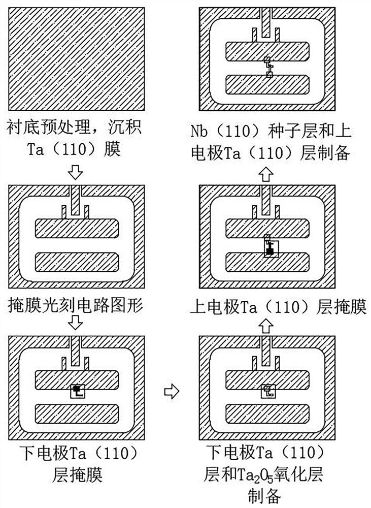
[0072] This embodiment provides a method for preparing a Josephson junction that meets the large wafer size. The lower electrode Ta (110) layer and the superconducting circuit pattern are formed step by step, such as figure 1 As shown, the preparation method specifically includes the following steps:

[0073] (I) Surface atomic step treatment, back pre-coating and active oxygen assisted surface cleaning are carried out on the substrate, Ta(110) film is deposited on the C-plane sapphire substrate, and superconducting circuit patterns are formed by photolithography. The Ta(110) film is made of Prepared by magnetron sputtering, the growth temperature is 500°C, the working pressure is 13mTorr, the DC power is 600W, the target base distance is 110mm, and the growth thickness is 100nm;

[0074] The lower electrode Ta (110) layer is prepared by mask photolithography in the overlapping area of ​​the superconducting circuit pattern, and the lower electrode Ta (110) layer is prepared by...

Embodiment 2

[0079] This embodiment provides a method for preparing a Josephson junction meeting a large wafer size. The lower electrode Ta (110) layer and the superconducting circuit pattern are formed step by step. The preparation method specifically includes the following steps:

[0080](I) Surface atomic step treatment, back pre-coating and active oxygen assisted surface cleaning are carried out on the substrate, Ta(110) film is deposited on the C-plane sapphire substrate, and superconducting circuit patterns are formed by photolithography. The Ta(110) film is made of Prepared by magnetron sputtering, the growth temperature is 410°C, the working pressure is 5mTorr, the DC power is 400W, the target base distance is 70mm, and the growth thickness is 50nm;

[0081] The lower electrode Ta (110) layer is prepared by mask photolithography in the overlapping area of ​​the superconducting circuit pattern, and the lower electrode Ta (110) layer is prepared by magnetron sputtering, including: fir...

Embodiment 3

[0086] This embodiment provides a method for preparing a Josephson junction meeting a large wafer size. The lower electrode Ta (110) layer and the superconducting circuit pattern are formed step by step. The preparation method specifically includes the following steps:

[0087] (I) Surface atomic step treatment, back pre-coating and active oxygen assisted surface cleaning are carried out on the substrate, Ta(110) film is deposited on the C-plane sapphire substrate, and superconducting circuit patterns are formed by photolithography. The Ta(110) film is made of Prepared by magnetron sputtering, the growth temperature is 600°C, the working pressure is 8mTorr, the DC power is 700W, the target base distance is 150mm, and the growth thickness is 150nm;

[0088] The lower electrode Ta (110) layer is prepared by mask photolithography in the overlapping area of ​​the superconducting circuit pattern, and the lower electrode Ta (110) layer is prepared by magnetron sputtering, including: ...


PUM

PropertyMeasurementUnit
Thicknessaaaaaaaaaa

Abstract

The invention provides a Josephson junction satisfying a large wafer size, a preparation method and an application. The Josephson junction is prepared by preparing a Ta (110) film on a substrate, preparing a superconducting circuit structure through photoetching, forming a lower electrode Ta (110) layer through mask photoetching, preparing a Ta2O5 oxide layer on the surface of the lower electrode Ta (110) layer as an intermediate layer, and forming an upper electrode Ta (110) layer through mask photoetching. The Ta (110) superconducting thin film is used as the lower electrode and the upper electrode of the Josephson junction, the Ta2O5 oxide layer on the surface of the Ta (110) superconducting thin film has the characteristics of compactness, stability and the like, passivation and optimization can be performed by adopting a piranha solution, photoetching residual glue is further removed, the stability of a superconducting circuit structure and the Josephson junction is ensured, the method has the characteristics of simple process steps, stability, controllability, high integration level and the like, and the method is suitable for large-scale production. Uniform and stable Josephson junctions in a large wafer size range can be prepared, and the method is suitable for regulation and control of Josephson junctions with different areas.

Description

technical field [0001] The invention belongs to the technical field of superconducting chips, and relates to a Josephson junction satisfying a large wafer size, a preparation method and an application. Background technique [0002] As the core basic component of quantum chips, the structure and fabrication process of superconducting Josephson junctions have been extensively studied. How to ensure and improve the performance of the Josephson junction and simplify its preparation process has become a research hotspot. At the same time, in order to promote the realization of universal quantum computing, it is also important to prepare a stable and scalable Josephson junction that meets the large wafer size. [0003] At present, the suspension gel structure and the double-tilt evaporation technology are still common techniques for preparing Josephson junctions. A typical example is based on aluminum (Al) / alumina (AlO x ) / Al superconducting Josephson junction. After long-term d...

Claims


Application Information

Patent Timeline
IPC IPC(8): H01L39/24H01L39/02H01L39/12H01L39/22
CPCH10N60/805H10N60/855H10N60/12H10N60/0912Y02E40/60
Inventor 杨丽娜冯加贵熊康林吴艳伏李睿颖贾浩林
Owner GUSU LAB OF MATERIALS
Why Eureka
Try Eureka