Inverted deep ultraviolet LED chip capable of increasing p-side reflection emergent light and manufacturing method of inverted deep ultraviolet LED chip
A technology of LED chips and manufacturing methods, which is applied in the direction of semiconductor devices, electrical components, circuits, etc., can solve the problems of deterioration of electrical performance of deep ultraviolet LEDs, achieve the effects of improving light extraction efficiency, enhancing reflectivity, and reducing defects
- Summary
- Abstract
- Description
- Claims
- Application Information
AI Technical Summary
Problems solved by technology
Method used
Image

Examples
Embodiment 1
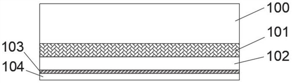
[0076] see Figure 1j , a flip-chip deep ultraviolet LED chip with increased p-side reflected light, its light-emitting part includes an epitaxial layer, a passivation layer 109, a p-electrode and an n-electrode that are sequentially stacked on the substrate 100, and the surface of the epitaxial layer includes A p-region, an n-region, and a second-order stepped structure, the second-order stepped structure is disposed between the p-region and the n-region and serves as a boundary between the p-region and the n-region;
[0077] The epitaxial layer corresponding to the p region includes an AlN buffer layer 101 , an n-A1GaN layer 102 , a quantum well layer 103 , a p-AlGaN layer 104 and a secondary grown p-GaN layer 106 , which are sequentially stacked on the substrate 100 . , the p-GaN layer 106 does not completely cover the p-AlGaN layer 104 below it, and the epitaxial layer corresponding to the n region includes an AlN buffer layer 101 and an n-AlGaN layer 102 stacked on the su...
Embodiment 2
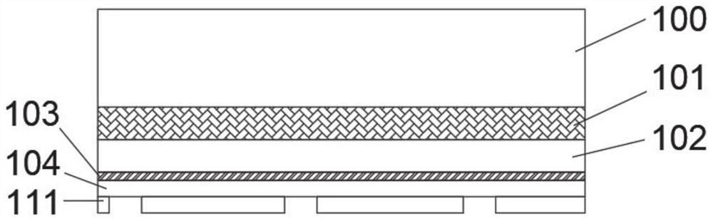
[0096] see Figure 2j , a flip-chip deep ultraviolet LED chip with increased p-side reflected light, its light-emitting part includes an epitaxial layer, a passivation layer 209, a p-electrode and an n-electrode whose bottom layer is sequentially arranged on the substrate 200, and the surface of the epitaxial layer includes p a region, an n-region, and a second-order stepped structure, the second-order stepped structure being disposed between the p-region and the n-region and serving as a boundary between the p-region and the n-region;
[0097] The epitaxial layer corresponding to the p region includes an AlN buffer layer 201 , an n-AlGaN layer 202 , a quantum well layer 203 , a p-AlGaN layer 204 and a secondary grown p-GaN layer 206 , which are sequentially stacked on the substrate 200 . , the p-GaN layer 206 does not completely cover the p-AlGaN layer 204 below it, and the epitaxial layer corresponding to the n region includes an AlN buffer layer 202 and an n-AlGaN layer 202...
Embodiment 3
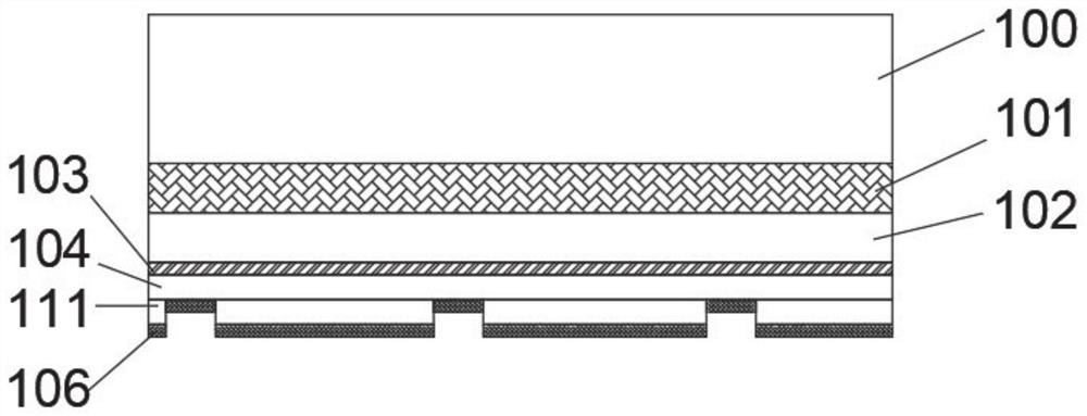
[0116] The structure and manufacturing method of a flip-chip deep ultraviolet LED chip with increased p-side reflected light in this embodiment 3 are basically the same as the device structure and manufacturing method in The chemical layer 109 is SiO grown by plasma enhanced chemical vapor deposition, atomic layer deposition or electron beam evaporation. 2 or Si 3 N 4 or Al 2 O 3 The passivation layer, corresponding to the passivation layer 309 in Example 3, is PI or SU-8 with a thickness of 4-6 μm formed by spin coating or spray coating and thermal curing.
[0117] The difference between a flip-chip deep ultraviolet LED chip manufacturing method that increases the p-side reflected light in Embodiment 3 and Embodiment 1 is only that the method of step S9 is different, and the details are as follows:
[0118] Step S9: coating the surfaces of the metal reflective electrode 108, the p-AlGaN layer 104, the n-AlGaN layer 102 and the n-type ohmic contact electrode 105 by means o...
PUM
| Property | Measurement | Unit |
|---|---|---|
| Thickness | aaaaa | aaaaa |
| Thickness | aaaaa | aaaaa |
| Thickness | aaaaa | aaaaa |
Abstract
Description
Claims
Application Information
 - Generate Ideas
- Intellectual Property
- Life Sciences
- Materials
- Tech Scout
- Unparalleled Data Quality
- Higher Quality Content
- 60% Fewer Hallucinations
Browse by: Latest US Patents, China's latest patents, Technical Efficacy Thesaurus, Application Domain, Technology Topic, Popular Technical Reports.
© 2025 PatSnap. All rights reserved.Legal|Privacy policy|Modern Slavery Act Transparency Statement|Sitemap|About US| Contact US: help@patsnap.com