Preparation method of carrier transport film and preparation method of quantum dot light-emitting diode

A quantum dot luminescence and carrier technology, which is applied in semiconductor/solid-state device manufacturing, semiconductor devices, electrical components, etc., can solve the problem of low carrier mobility, reduce roughness, improve microscopic appearance, film The effect of layer crystallinity improvement

Pending Publication Date: 2022-07-01
TCL CORPORATION
View PDF0 Cites 0 Cited by
  • Summary
  • Abstract
  • Description
  • Claims
  • Application Information

AI Technical Summary

Problems solved by technology

[0006] The purpose of this application is to provide a method for preparing a carrier transport film and a method for preparing a quantum dot light-emitting diode, aiming to solve the technical problem that the carrier mobility of the carrier transport film is not high

Method used


Image

  • Preparation method of carrier transport film and preparation method of quantum dot light-emitting diode
  • Preparation method of carrier transport film and preparation method of quantum dot light-emitting diode
  • Preparation method of carrier transport film and preparation method of quantum dot light-emitting diode

Examples


preparation example Construction

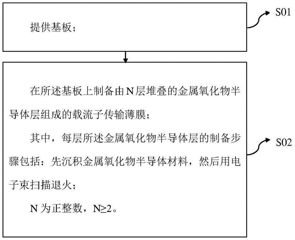
[0028] A first aspect of the embodiments of the present application provides a method for preparing a carrier transport film, such as figure 1 shown, including the following steps:

[0029] S01: Provide substrate;

[0030] S02: prepare a carrier transport film composed of N-layer stacked metal oxide semiconductor layers on the substrate;

[0031] Wherein, the preparation steps of each metal oxide semiconductor layer include: first depositing metal oxide semiconductor material, and then scanning annealing with electron beam;

[0032] N is a positive integer, N≥2.

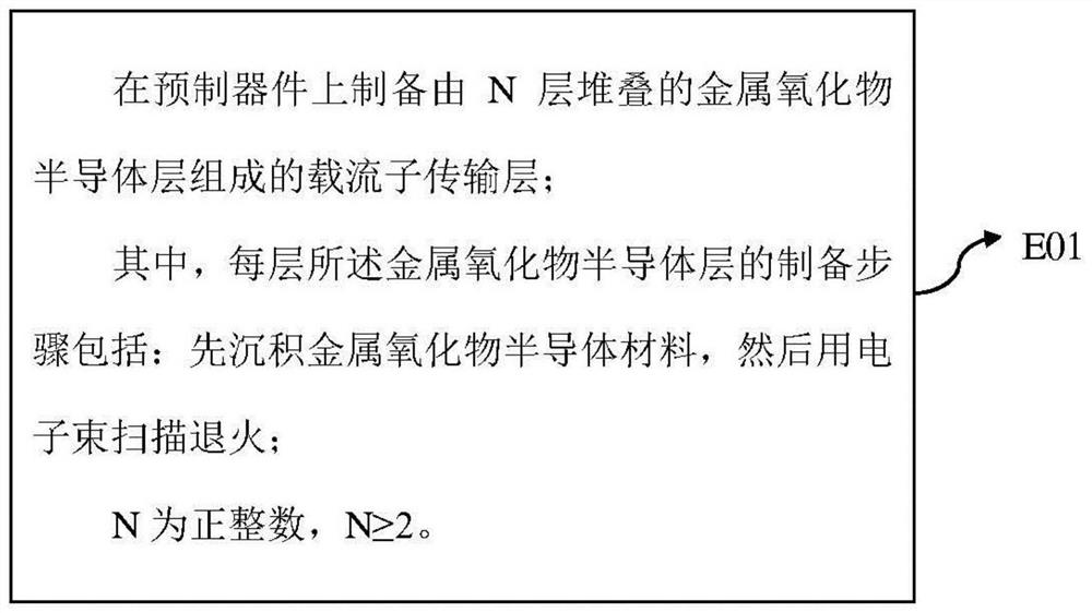
[0033] The preparation method of the carrier transport film provided by the present application adopts the technology of N-layer metal oxide semiconductor layer stacking and layering preparation, that is, each metal oxide semiconductor layer is firstly deposited metal oxide semiconductor material, and then electron beam Scanning annealing; such a preparation method can improve the microscopic morphology of the car...

Embodiment 1

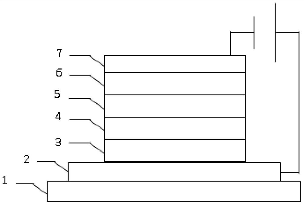
[0090] An upright quantum dot light-emitting diode, from bottom to top, comprises: an ITO substrate (anode), a hole injection layer, a hole transport layer, a quantum dot light-emitting layer, an electron transport layer, and a cathode. Its preparation process includes the following steps:

[0091] Step S1: on the ITO substrate (anode), spin-coating PEDOT:PSS at a rotational speed of 5000 rpm and a time of 30 seconds, followed by heating at 150° C. for 15 minutes, and standing to cool for 5 minutes to obtain a hole injection layer.

[0092] Step S2: spin-coating TFB (8 mg / mL) on the above hole injection layer with a rotational speed of 3000 rpm and a time of 30 seconds, followed by heating at 80° C. for 10 minutes, and standing to cool for 5 minutes to obtain hole transport Floor.

[0093] Step S3: spin-coating quantum dots (20 mg / mL) on the hole transport layer under the conditions of a rotational speed of 2000 rpm and a time of 30 seconds to obtain a quantum dot light-emitt...

Embodiment 2

[0102] An upright quantum dot light-emitting diode, from bottom to top, comprises: an ITO substrate (anode), a hole injection layer, a hole transport layer, a quantum dot light-emitting layer, an electron transport layer, and a cathode. Its preparation process includes the following steps:

[0103] Step S1: on the ITO substrate (anode), spin-coating PEDOT:PSS at a rotational speed of 5000 rpm and a time of 30 seconds, followed by heating at 150° C. for 15 minutes, and standing to cool for 5 minutes to obtain a hole injection layer.

[0104] Step S2: spin-coating TFB (8 mg / mL) on the above hole injection layer with a rotational speed of 3000 rpm and a time of 30 seconds, followed by heating at 80° C. for 10 minutes, and standing to cool for 5 minutes to obtain hole transport Floor.

[0105] Step S3: spin-coating quantum dots (20 mg / mL) on the hole transport layer under the conditions of a rotational speed of 2000 rpm and a time of 30 seconds to obtain a quantum dot light-emitt...


PUM

PropertyMeasurementUnit
Power densityaaaaaaaaaa
Thicknessaaaaaaaaaa
Energy densityaaaaaaaaaa

Abstract

The invention relates to the technical field of display devices, and provides a preparation method of a fluid transmission film, which comprises the following steps: providing a substrate; preparing a carrier transport film formed by N stacked metal oxide semiconductor layers on the substrate; wherein each metal oxide semiconductor layer is prepared by the following steps of: firstly depositing a metal oxide semiconductor material, and then scanning and annealing by using an electron beam; n is a positive integer greater than or equal to 2. According to the preparation method, the microstructure of the carrier transport thin film can be improved, the roughness of the carrier transport thin film is reduced, the film layer is smoother, the crystallinity of the film layer is improved, the molecular arrangement is more orderly, and the carrier mobility is finally improved.

Description

technical field [0001] The application belongs to the technical field of display devices, and in particular relates to a preparation method of a carrier transport film and a preparation method of a quantum dot light-emitting diode. Background technique [0002] Quantum Dots Light-Emitting Diode (QLED) is an emerging display device, its structure is similar to organic light-emitting diode (Organic Light-Emitting Diode, OLED), it has a sandwich structure, and its light-emitting layer is composed of quantum dots ( Quantum Dot, QD) composition. Quantum dots are particles with a particle diameter of less than 10nm. This substance has a very special property: when quantum dots are stimulated by photoelectricity, they emit colored light. Shape decides. Because of this property, it is able to change the color of the light emitted by the light source. The light-emitting wavelength range of quantum dots is very narrow, the color is relatively pure, and it can be adjusted, so the pi...

Claims


Application Information

Patent Timeline
IPC IPC(8): H01L51/56H01L51/50H01L51/54
CPCH10K71/421H10K50/115H10K50/156H10K50/166H10K2102/00H10K71/00
Inventor 敖资通严怡然张建新杨帆赖学森洪佳婷
Owner TCL CORPORATION
Why Eureka
Try Eureka