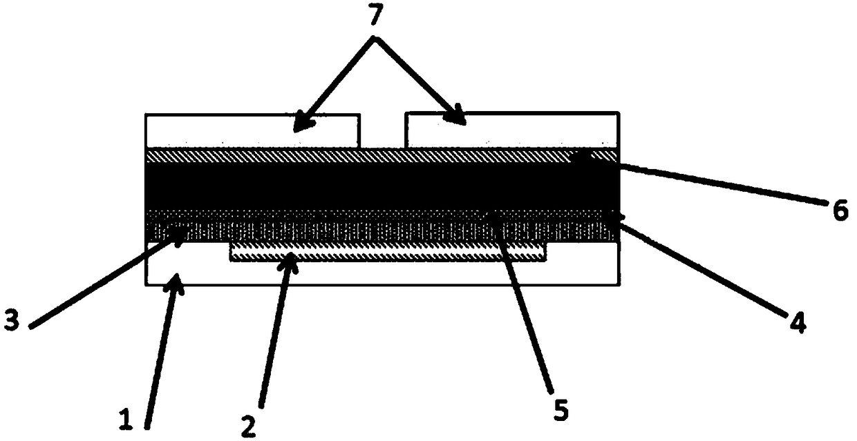
Perovskite solar cell using titanium oxide and barium titanate composite material as electron transfer layer and its preparation method
A technology of electron transport layer and solar cell, which is applied in the field of solar cells, can solve the problems of poor contact between the perovskite light absorption layer and the electron transport layer, and the inability to form the perovskite light absorption layer, so as to improve the photoelectric characteristics and improve Effects of Microscopic Morphology and Performance Improvement
- Summary
- Abstract
- Description
- Claims
- Application Information
AI Technical Summary
Problems solved by technology
Method used
Image
Examples
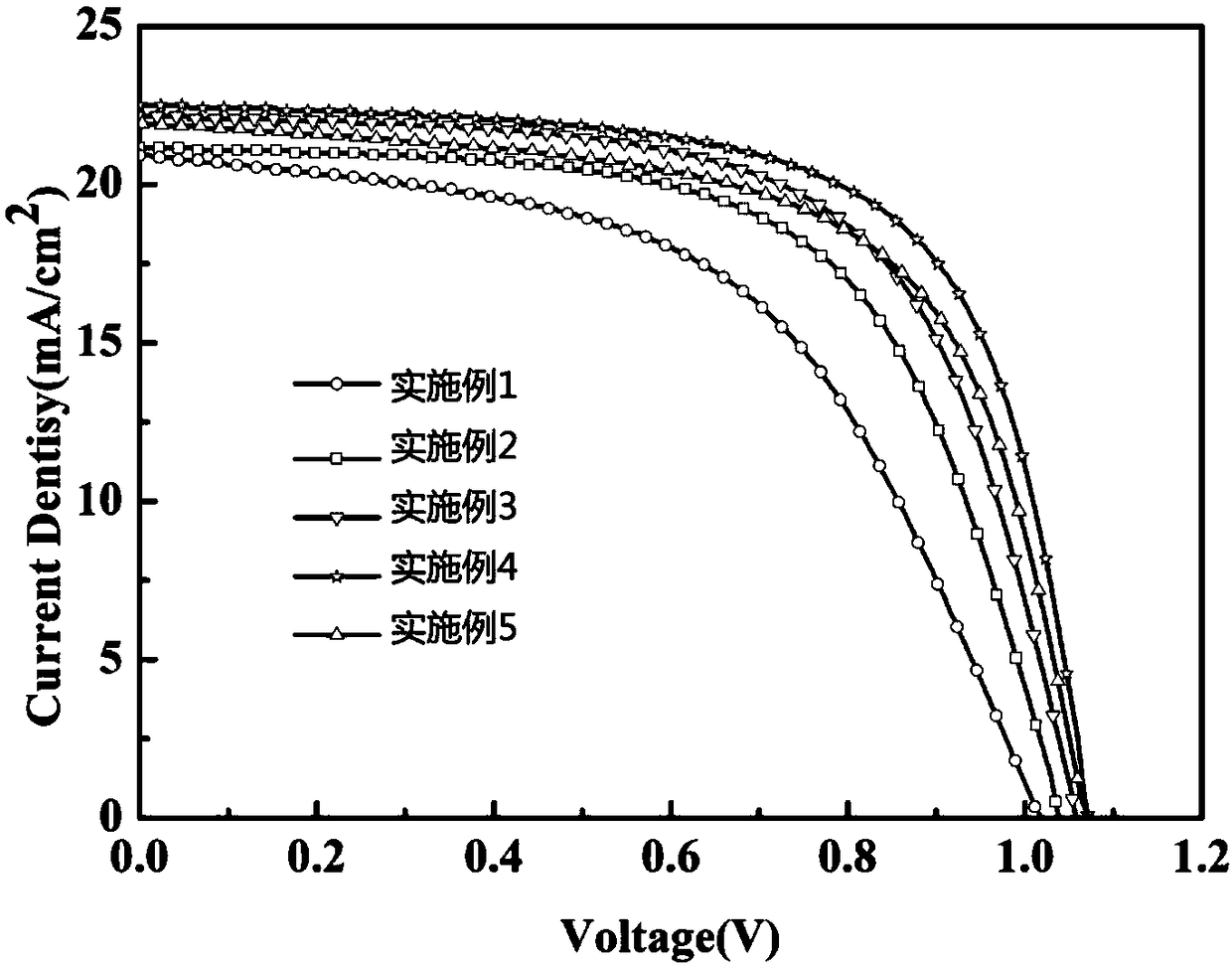
Embodiment 1
[0027] ① First, clean the FTO conductive glass, put the glass in toluene, acetone, deionized water, isopropanol and ultrasonically treat it for 20 minutes, and then use nitrogen to dry the glass for later use;
[0028] ②Configure 0.15mol / L titanium acetylacetonate solution, the solvent is n-butanol, stir the titanium acetylacetonate solution evenly;
[0029] ③ Spin-coat the titanium acetylacetonate solution in step ② on the spare FTO conductive glass in step ① using a homogenizer, then use a heating plate to heat the glass substrate at 130°C for 5 minutes, and then use a muffle furnace to The glass substrate was heated at 500°C for 30 minutes, and after cooling, an electron transport layer with only titanium oxide was formed, with a thickness of about 60 nanometers;
[0030] ④ Configure the perovskite solution. The specific operation is: mix DMF (dimethylformamide) and DMSO (dimethyl sulfoxide) at a volume ratio of 9:1 and stir evenly, then add CH 3 NH 3 I and PbI 2 Mix and...
Embodiment 2
[0035] ① First, clean the FTO conductive glass, put the glass in toluene, acetone, deionized water, isopropanol in turn and ultrasonically treat it for 20 minutes, then use nitrogen to dry the glass for later use;
[0036] ② Configure 0.15mol / L titanium acetylacetonate solution, the solvent is n-butanol. Stir the titanium acetylacetonate solution evenly;
[0037]③ Spin-coat the titanium acetylacetonate solution in step ② on the spare FTO conductive glass in step ① using a homogenizer, then use a heating plate to heat the glass substrate at 130°C for 5 minutes, and then use a muffle furnace to The glass substrate was heated at 500°C for 30 minutes, cooled and then used for later use;
[0038] ④ Configure 0.015mol / L Ba(NO 3 ) 2 aqueous solution and Ba(NO 3 ) 2 The solution was stirred evenly.
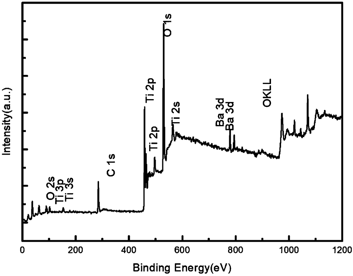
[0039] ⑤Take 100mL of Ba(NO 3 ) 2 The solution was placed in a beaker, and the glass substrate spared in step ③ was soaked in Ba(NO 3 ) 2 solution for 30 seconds, then use deion...
Embodiment 3
[0045] Embodiment 3 is basically the same as Embodiment 2, the difference is:
[0046] After step ⑤, repeat step ⑤ again, and the thickness of the obtained electron transport layer is 60 nanometers.
PUM
| Property | Measurement | Unit |
|---|---|---|
| Thickness | aaaaa | aaaaa |
| Thickness | aaaaa | aaaaa |
| Thickness | aaaaa | aaaaa |
Abstract
Description
Claims
Application Information


