Epitaxial wafer preparation method, epitaxial wafer and ultraviolet light-emitting diode

An epitaxial wafer, quantum technology, applied in the semiconductor field, can solve the problem of low quantum efficiency, and achieve the effect of increasing hole concentration, improving internal quantum efficiency, and blocking electron overflow

Pending Publication Date: 2022-07-15
JIANGXI ZHAO CHI SEMICON CO LTD
View PDF0 Cites 3 Cited by
  • Summary
  • Abstract
  • Description
  • Claims
  • Application Information

AI Technical Summary

Problems solved by technology

[0004] In view of this, the purpose of the present invention is to provide a method for preparing epitaxial wafers, epitaxial wafers and ultraviolet light-emitting diodes, aiming at solving the problem of low quantum efficiency in the prior art epitaxial wafers

Method used


Image

  • Epitaxial wafer preparation method, epitaxial wafer and ultraviolet light-emitting diode
  • Epitaxial wafer preparation method, epitaxial wafer and ultraviolet light-emitting diode
  • Epitaxial wafer preparation method, epitaxial wafer and ultraviolet light-emitting diode

Examples


Embodiment 1

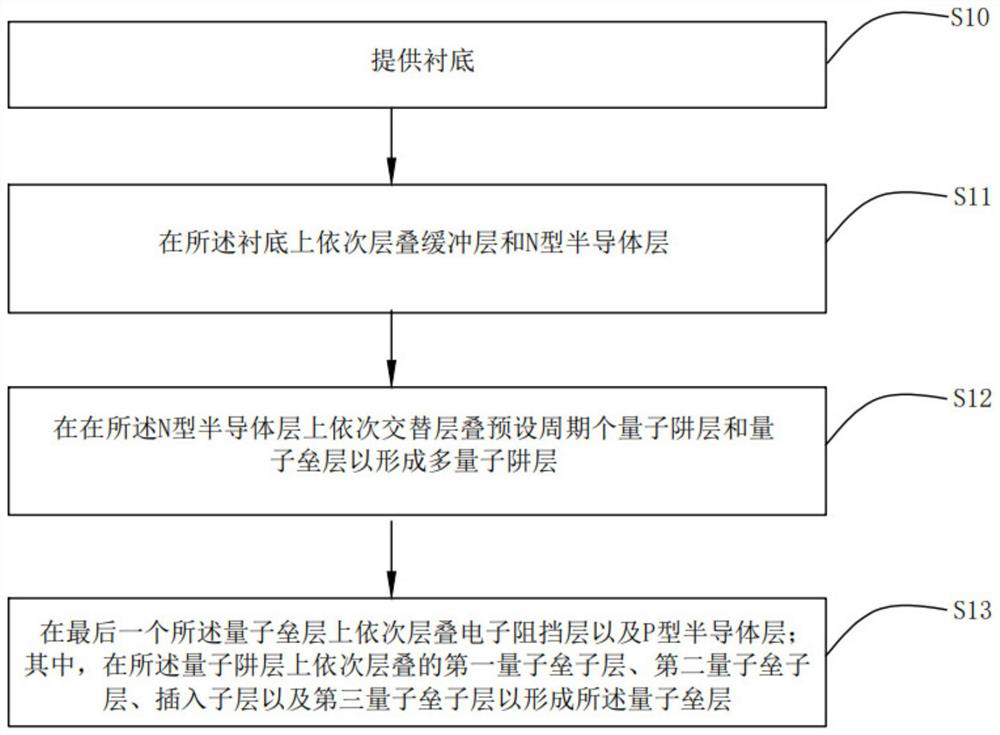
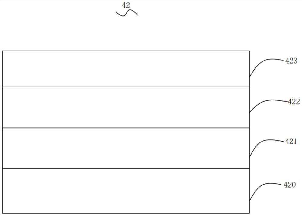
[0034] see figure 1 , is the method for preparing an epitaxial wafer proposed in the first embodiment of the present invention, and the method for preparing an epitaxial wafer includes steps S10 to S11 .

[0035] Step S10, providing a substrate.

[0036] Among them, the substrate includes but is not limited to sapphire, SiC, Si-based, and GaN. In this embodiment, the substrate is a Si-based substrate. The Si-based substrate has the advantages of good thermal conductivity, low cost, mature technology, and easy peeling. .

[0037] In step S11, a buffer layer and an N-type semiconductor layer are sequentially stacked on the substrate.

[0038] Specifically, in this embodiment, the buffer layer adopts an AlN layer.

[0039] Step S12, sequentially stacking a predetermined period of quantum well layers and quantum barrier layers alternately on the N-type semiconductor layer to form multiple quantum well layers.

[0040] The number of preset cycles can be set according to actual ...

Embodiment approach

[0048] More specifically, in order to clearly understand the specific implementation process of the present invention, the specific growth process of the entire epitaxial wafer is described in detail below, which is an embodiment of the present invention, but the growth process of the epitaxial wafer of the present invention is not limited to this. It does not constitute a limitation of the present invention.

[0049] Put the substrate in the MOCVD reaction chamber, pass TMAl and NH into the reaction chamber 3 , AlN layer is obtained by preparing AlN thin film by chemical vapor deposition method. Specifically, in this embodiment, the growth temperature of the AlN layer is 1250°, the growth thickness is about 1.5 μm, and the growth pressure is 50 mbar.

[0050] The main purpose of growing the high temperature AlN layer is to release the lattice mismatch and thermal mismatch between the substrate and the AlGaN material. Therefore, in this embodiment, the layer adopts NH under t...

Embodiment 2

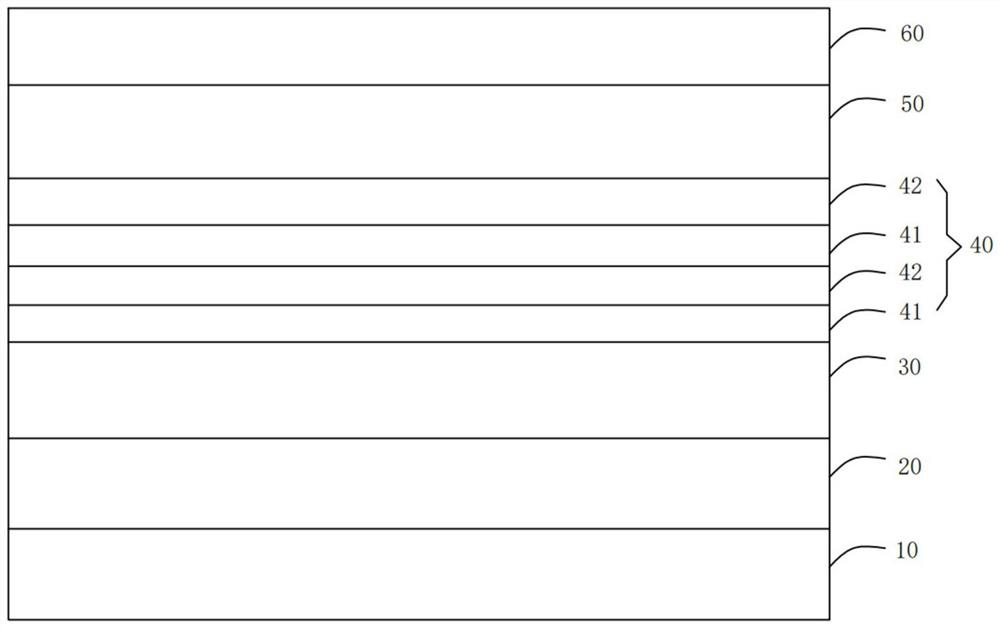
[0057] see Figure 2 to Figure 3 , shows the epitaxial wafer proposed in the first embodiment of the present invention, the epitaxial wafer is prepared by the epitaxial wafer preparation method in the above-mentioned first embodiment, and the epitaxial wafer includes:

[0058] The substrate 10 , the buffer layer 20 , the N-type semiconductor layer 30 , the multiple quantum well layer 40 , the electron blocking layer 50 and the P-type semiconductor layer 60 epitaxially grown on the substrate 10 in sequence.

[0059] Preferably, the buffer layer is an AlN layer, and the N-type semiconductor layer 30 is N-type doped Al x Ga (1-x) N layer, the electron blocking layer 50 is Al y Ga (1-y) N layer, P-type semiconductor layer 60 is P-type doped Al z Ga (1-z) N layers.

[0060] The multiple quantum well layer 40 includes quantum well layers 41 and quantum barrier layers 42 that are alternately stacked periodically. Specifically, the number of periods can be set according to the a...


PUM

PropertyMeasurementUnit
thicknessaaaaaaaaaa
thicknessaaaaaaaaaa

Abstract

The invention discloses an epitaxial wafer preparation method, an epitaxial wafer and an ultraviolet light-emitting diode. The epitaxial wafer preparation method comprises the following steps: providing a substrate; sequentially laminating a buffer layer and an N-type semiconductor layer on the substrate; sequentially and alternately laminating quantum well layers and quantum barrier layers of a preset period on the N-type semiconductor layer to form a multi-quantum well layer; an electron barrier layer and a P-type semiconductor layer are sequentially stacked on the last quantum barrier layer; wherein a first quantum barrier sub-layer, a second quantum barrier sub-layer, an insertion sub-layer and a third quantum barrier sub-layer are sequentially stacked on the quantum well layer to form a quantum barrier layer, the quantum well layer, the first quantum barrier sub-layer, the second quantum barrier sub-layer and the third quantum barrier sub-layer are all AlGaN layers, the insertion sub-layer is an MgN layer, and the third quantum barrier sub-layer is an AlGaN layer. The Al component content of the first quantum barrier sub-layer and the Al component content of the third quantum barrier sub-layer are both lower than the Al component content of the second quantum barrier sub-layer. By adopting the epitaxial wafer, the problem of low quantum efficiency in the epitaxial wafer in the prior art can be solved.

Description

technical field [0001] The invention relates to the technical field of semiconductors, in particular to a method for preparing an epitaxial wafer, an epitaxial wafer and an ultraviolet light emitting diode. Background technique [0002] Ultraviolet LEDs generally refer to LEDs with a central wavelength of light below 400 nm. Because of their unique wavelength characteristics, they are widely used in biomedical, anti-counterfeiting identification, purification fields (such as water purification, air purification, etc.), computer data storage and military. Moreover, with the development of technology, new applications will continue to appear to replace the original technologies and products, and UV LEDs have broader market application prospects. Therefore, it is particularly important to develop UV LEDs with better performance. [0003] However, compared with GaN-based blue LEDs, the development of UV LEDs faces many unique technical difficulties, such as: the higher the Al co...

Claims


Application Information

Patent Timeline
Patent Type & Authority Applications(China)
IPC IPC(8): H01L33/00C30B25/02C30B29/38C30B29/40H01L33/06H01L33/14H01L33/32
CPCH01L33/06H01L33/007H01L33/145H01L33/325C30B29/38C30B29/403C30B25/02
Inventor 刘春杨胡加辉吕蒙普金从龙
Owner JIANGXI ZHAO CHI SEMICON CO LTD
Why Eureka
Try Eureka