Preparation method of solder for eutectic bonding of bulge structure
A technology of eutectic bonding and solder, which is applied in semiconductor/solid-state device manufacturing, semiconductor/solid-state device components, semiconductor devices, etc., can solve the problem of smaller spacing between adjacent raised structures, and improve the bonding effect, Effect of avoiding metal solder loss
- Summary
- Abstract
- Description
- Claims
- Application Information
AI Technical Summary
Problems solved by technology
Method used
Image

Examples
preparation example Construction
[0024] Since the prior art prepares the adhesion layer and the seed layer of the eutectic bonding solder on the top of the bump structure, metal is also sputtered on the sidewall of the bump structure, so that when the metal solder is formed by electroplating, the sidewall is Metal solder also grows. In order to avoid the formation of metallic solder on the sidewalls of the raised structures, the present invention provides an improved method for preparing solder for eutectic bonding, which includes the following steps.
[0025] First, a substrate is provided, the substrate is provided with raised structures, and the top surfaces of the raised structures are bonding surfaces.
[0026] The substrate of the present invention can be a silicon wafer, a silicon-on-insulator wafer, a silicon-germanium wafer, a germanium wafer, a gallium nitride wafer, a SiC wafer, a quartz wafer or a sapphire wafer. The present invention has no particular limitation on the substrate, and conventiona...
Embodiment 1
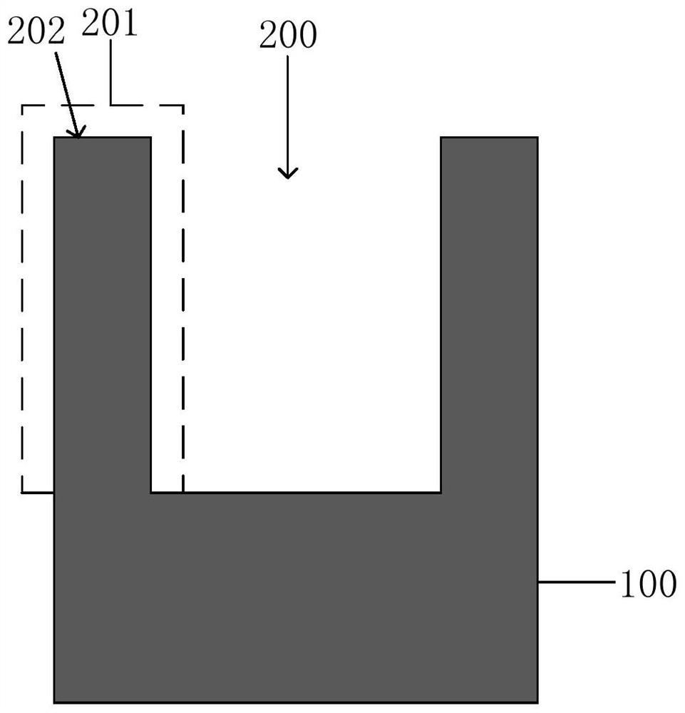
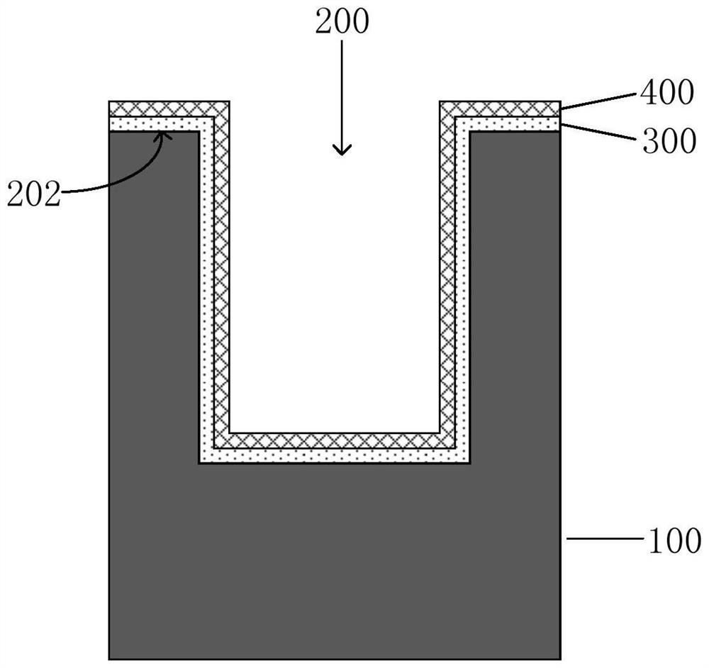
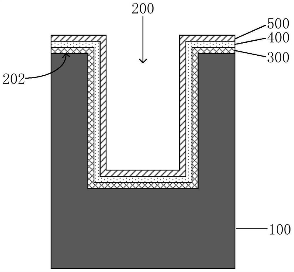
[0056] First, a silicon wafer 100 is provided. Then, a microchannel 200 is formed on the upper surface of the silicon wafer 100 by photolithography and etching, and a schematic diagram of the partial structure of the obtained structure is shown in figure 1 As shown, 201 is the spacer wall of the microchannel 200 , and 202 is the bonding surface on the top of the spacer wall 201 .
[0057] Then, an adhesion layer 300 is formed by sputtering to cover the bonding surface 202 and the inner wall of the microchannel 200 , wherein the adhesion layer 300 is titanium with a thickness of 100 nanometers.
[0058] After that, the seed layer 400 is formed on the upper surface of the adhesion layer 300 by sputtering, and the partial structure diagram of the obtained structure is shown in figure 2 As shown, the seed layer 400 is gold with a thickness of 200 nanometers.
[0059] Next, a metal barrier layer 500 is formed on the upper surface of the seed layer 400 by sputtering, and the par...
PUM
| Property | Measurement | Unit |
|---|---|---|
| Thickness | aaaaa | aaaaa |
| Thickness | aaaaa | aaaaa |
| Thickness | aaaaa | aaaaa |
Abstract
Description
Claims
Application Information
 - Generate Ideas
- Intellectual Property
- Life Sciences
- Materials
- Tech Scout
- Unparalleled Data Quality
- Higher Quality Content
- 60% Fewer Hallucinations
Browse by: Latest US Patents, China's latest patents, Technical Efficacy Thesaurus, Application Domain, Technology Topic, Popular Technical Reports.
© 2025 PatSnap. All rights reserved.Legal|Privacy policy|Modern Slavery Act Transparency Statement|Sitemap|About US| Contact US: help@patsnap.com