LED epitaxial structure and preparation method thereof

An epitaxial structure and sub-layer technology, applied in semiconductor devices, electrical components, circuits, etc., can solve problems such as affecting radiation recombination efficiency, affecting luminous efficiency, limiting concentration, etc.

Active Publication Date: 2022-07-29
JIANGXI ZHAO CHI SEMICON CO LTD
View PDF5 Cites 3 Cited by
  • Summary
  • Abstract
  • Description
  • Claims
  • Application Information

AI Technical Summary

Problems solved by technology

[0005] In order to solve the above technical problems, the present invention provides an LED epitaxial structure and its preparation method, which is used to solve the problem that most of the effective electron-hole recombination occurs in the last few quantum wells of the multi-quantum wells in the prior art, so that the effective The radiation recombination luminous area is small, which affects the luminous efficiency. At the same time, the ionization energy of Mg doping is high, which limits the concentration of holes in P-type GaN, thereby affecting the technical problem of radiation recombination efficiency.

Method used


Image

  • LED epitaxial structure and preparation method thereof
  • LED epitaxial structure and preparation method thereof
  • LED epitaxial structure and preparation method thereof

Examples


Embodiment 1

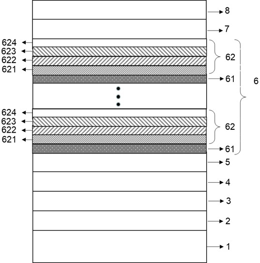
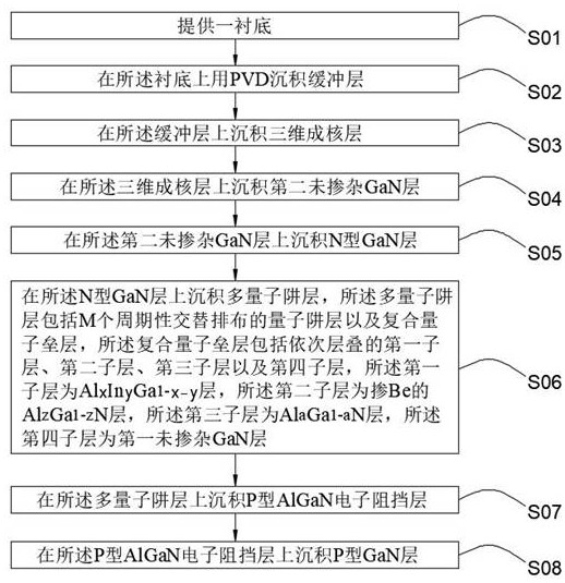
[0038] likefigure 1 As shown, the first embodiment of the present invention provides an LED epitaxial structure, including:

[0039] The substrate 1, the first semiconductor layer, the multiple quantum well layer 6 and the second semiconductor layer are stacked in sequence, and the multiple quantum well layer includes M periodically alternately arranged quantum well layers 61 and composite quantum barrier layers 62;

[0040] Wherein, the quantum well layer 61 is In b Ga 1-b N layers, the composite quantum barrier layer 62 includes a first sub-layer, a second sub-layer, a third sub-layer and a fourth sub-layer stacked on the quantum well layer in sequence, and the first sub-layer is Al x In y Ga 1-x-y N layer 621, the second sublayer is Be-doped Al z Ga 1-z N layer 622, the third sublayer is Al a Ga 1-a The N layer 623, the fourth sublayer is the first undoped GaN layer 624, the doping concentration of Be and the Al composition in the second sublayer are both directed to...

Embodiment 2

[0061] The second embodiment of the present invention provides an LED epitaxial structure. The LED epitaxial structure provided in the second embodiment is the same as that of the first embodiment, but the difference is as follows: the quantum well layers 61 and the composite quantum barrier layers 62 are alternately arranged. The value range of the period M is: 8≤M≤10, and the specific M is 9, that is, the quantum well layer 61 and the composite quantum barrier layer 62 are alternately grown 9 times to obtain the multi-quantum well layer 6;

[0062] The larger the period of the quantum well layer 61 and the composite quantum barrier layer 62 is, the easier it is for electrons and holes to be trapped, but the crystal quality of InGaN is worse than that of GaN, because the equilibrium vapor pressure of InN is the highest among all III-VI, In order to ensure the equilibrium vapor pressure of N, a higher temperature is required to crack NH 3 However, because the In-N bond is weak...

Embodiment 3

[0064] The third embodiment of the present invention provides an LED epitaxial structure. The LED epitaxial structure provided in the third embodiment is the same as that of the first embodiment, but the difference is as follows: the quantum well layers 61 and the composite quantum barrier layers 62 are alternately arranged. The value range of the period M is: 8≤M≤10, and the specific M is 10, that is, the quantum well layer 61 and the composite quantum barrier layer 62 are alternately grown 10 times to form the multiple quantum well layer 6 .

[0065] When M is larger, electrons and holes are more easily captured, but the crystal quality of InGaN is worse than that of GaN, because the equilibrium vapor pressure of InN is the highest among all III-VI. To ensure the equilibrium vapor pressure of N, a higher temperature is required split NH 3 However, because the In-N bond is weak and easy to break, it sometimes leads to the desorption of In atoms from the growth surface or the ...


PUM

PropertyMeasurementUnit
thicknessaaaaaaaaaa
thicknessaaaaaaaaaa
thicknessaaaaaaaaaa

Abstract

The invention provides an LED epitaxial structure and a preparation method thereof. An epitaxial wafer comprises a substrate, a first semiconductor layer, a multi-quantum well layer and a second semiconductor layer, the multi-quantum well layer comprises a quantum well layer and a composite quantum barrier layer; the composite quantum barrier layer comprises a Be-doped Al < z > Ga < 1-z > N layer, and the doping concentration of Be and the Al component in the Al < z > Ga < 1-z > N layer are gradually increased in the direction from the N-type GaN layer to the P-type GaN layer, so that the problems that in the prior art, effective electron hole recombination mostly occurs in the last few quantum wells of the multiple quantum wells, the effective radiation recombination light-emitting area is small, the light-emitting efficiency is influenced, and the light-emitting efficiency is influenced are solved. Meanwhile, Mg doping ionization energy is high, the concentration of holes in P-type GaN is limited, and then radiation recombination efficiency is affected.

Description

technical field [0001] The invention belongs to the technical field of LED epitaxy design, and in particular relates to an LED epitaxy structure and a preparation method thereof. Background technique [0002] LED (Light Emitting Diode, light-emitting diode) has the advantages of energy saving, environmental protection, long life, etc., and is the third generation of electric lighting sources after incandescent lamps and fluorescent lamps. The existing GaN-based LED epitaxial wafer includes a substrate, and a low temperature buffer layer, a three-dimensional nucleation layer, an undoped GaN layer, an N-type GaN layer, a multiple quantum well layer, an electron blocking layer and a P type GaN layer, wherein the multiple quantum well layer includes alternately grown InGaN well layers and GaN barrier layers, and the electron blocking layer (EBL) is a P-type AlGaN layer. [0003] Since the migration rate of electrons is much greater than that of holes, even with the existence of...

Claims


Application Information

Patent Timeline
Patent Type & Authority Applications(China)
IPC IPC(8): H01L33/06H01L33/32H01L33/00
CPCH01L33/06H01L33/325H01L33/0075H01L33/0066
Inventor 罗文博肖崇武张铭信陈铭胜
Owner JIANGXI ZHAO CHI SEMICON CO LTD
Why Eureka
Try Eureka