Flat shape electronic component and its mfg. method

An electronic component and sheet-like technology, applied in electrical components, inductance/transformer/magnet manufacturing, coil manufacturing, etc., can solve problems such as broken wires, internal conductor vibration, metal fatigue, etc.

Inactive Publication Date: 2004-06-23
TAIYO YUDEN KK
View PDF0 Cites 2 Cited by
  • Summary
  • Abstract
  • Description
  • Claims
  • Application Information

AI Technical Summary

Problems solved by technology

[0006] However, in the manufacturing process of the above-mentioned chip-shaped electronic components, when the sheet-shaped laminate is fired at high temperature to form a unit body, the firing shrinkage of the laminate is uneven, and there is a gap between adjacent ceramic plates inside the laminate. Occasionally, peeling (delamination) occurs between the ceramic plate and the internal conductor, and a void will be formed at the peeled part
[0007] Furthermore, at least one side of the inner conductor adjacent to this gap loses the support of the ceramic plate and becomes in a floating state. Therefore, when an impact is applied to the unit body from the outside, the inner conductor vibrates in the gap and metal fatigue occurs. thus the problem of disconnection
[0008] Especially in the case where the chip electronic component is an inductor, if a high-frequency current flows through the inner conductor, the surrounding magnetic body acts on the inner conductor with a violently changing electromagnetic force, and the inner conductor is subjected to this electromagnetic force in the gap. Vibration, will produce large metal fatigue, so there is a problem of disconnection

Method used


Image

  • Flat shape electronic component and its mfg. method
  • Flat shape electronic component and its mfg. method
  • Flat shape electronic component and its mfg. method

Examples


Embodiment 1

[0027] First, Fe was weighed at the following compounding ratio (mole %) (mol%) 2 o 3 , NiO, ZnO and CuO powders, adding water and stirring them with a ball mill for 15 hours, spraying and drying them with a spray dryer to obtain mixed powders.

[0028] Oxide type Mixing ratio

[0029] Fe 2 o 3 49mol%

[0030] NiO 35mol%

[0031] ZnO 10mol%

[0032] CuO 6mol%

[0033] Next, the mixed powder was calcined at 800° C. for 1 hour, and the obtained calcined product was put into a ball mill, and water was added to pulverize it for 15 hours. Then, the obtained slurry was spray-dried with a spray dryer to obtain a calcined product powder.

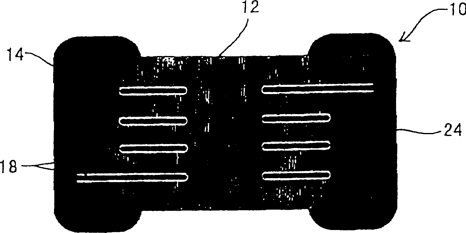
[0034] Next, the powder was stirred with an organic binder and an organic solvent, and a ferrite printed circuit board with a thickness of 50 μm was produced by using the obtained slurry by a doctor blade method.

[0035] Next, a plurality of through holes are formed at predetermined positions on the ferrite printed cir...

Embodiment 2

[0053] A unit body was formed in the same manner as in Example 1.

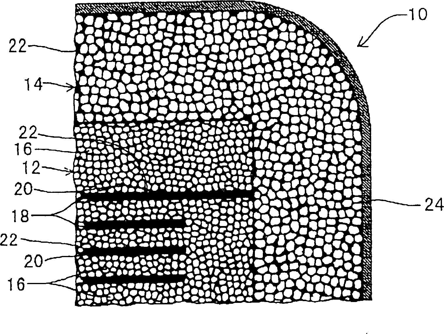
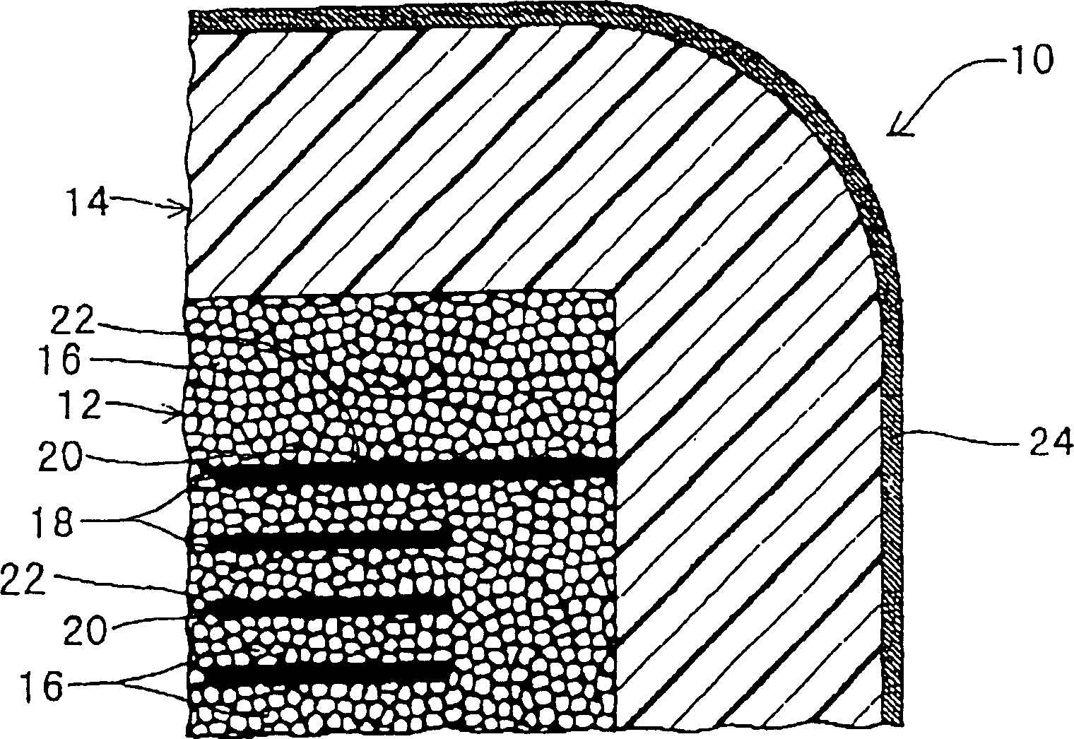
[0054] Next, put silicone resin diluted with toluene into the container, put the above-mentioned unit body in the silicone resin liquid, put the container into a decompression container, and depressurize it to 3.99966×10 with a vacuum pump. 3 Pa, keep in this state for about 10 minutes. Through this process, the gap between the magnetic body and the internal conductor is impregnated with the resin solution.

[0055] Next, this unit body was taken out of the container, and heated at 200° C. for 1 hour to harden the silicone resin impregnated in the cavity.

[0056] Next, put it in the rotating cylinder, and remove the synthetic resin adhering to the lead-out part of the inner conductor.

[0057] Next, a thermosetting epoxy resin-based conductive paste was applied to both ends of the unit body, and heated at 150°C for 60 minutes and 200°C for 30 minutes to harden. Furthermore, electroplating is applied to the...


PUM

PropertyMeasurementUnit
thicknessaaaaaaaaaa

Abstract

Delamination in the conventional chip-type electronic part may create voids thereinside, allowing an internal electrode therein to vibrate in presence of external impacts or large electromagnetic forces caused by a high frequency current flowing inside the electrode, in such a way that fatigue may accumulate in the internal electrode, which eventually will results in the internal electrode being electrically disconnected. To solve this problem, a chip-type electronic part of the present invention includes synthetic resins impregnated into the voids to secure the internal electrode, wherein external electrodes of the chip-type electronic part are made of a conductive synthetic resin or a porous conductive material formed by sintering a conductive paste. The former is achieved by impregnating the synthetic resins before the formation of the external electrodes and the later, by extending the pores from surfaces of the external electrodes to surfaces of a main body and then by impregnating the synthetic resins thereinto.

Description

technical field [0001] The present invention relates to chip electronic components such as chip inductors, chip capacitors, and LC composite chip components, and their manufacturing methods. Background technique [0002] A chip electronic component generally consists of a chip unit body as the body of the electronic component and a pair of external electrodes formed at the ends of the unit body. The unit body is composed of a magnetic constituent object and a sheet-shaped inner conductor arranged inside the magnetic constituent object. The end of the internal conductor is exposed at the end of the unit body, the external electrode is arranged at the end of the unit body, and the external electrode and the internal electrode are electrically connected here. [0003] When the chip electronic component is a chip inductor, the magnetic component system is composed of a magnetic body, and the internal conductor is generally formed in a spiral shape inside the magnetic component....

Claims


Application Information

Patent Timeline
Patent Type & Authority Patents(China)
IPC IPC(8): H01F17/00H01F27/29H01F41/00H01F41/04H01G4/12H01G4/228H01G4/232H01G4/252
CPCH01G4/232H01F27/292H01F41/043H01F41/005H01F17/0013H01G4/12
Inventor 岩尾秀美荒井真弓星健一中泽睦士
Owner TAIYO YUDEN KK
Why Eureka
Try Eureka