Method of contact printing on gold coated films

A film and polymer film technology, applied in the field of micro-contact printing, can solve the problems of insufficient bonding and hindering self-integration of monolayers

Inactive Publication Date: 2000-02-09
KIMBERLY-CLARK WORLDWIDE INC
View PDF0 Cites 3 Cited by
  • Summary
  • Abstract
  • Description
  • Claims
  • Application Information

AI Technical Summary

Problems solved by technology

In addition, the silicon must be treated with an adhesion promoter such as Cr or Ti in a separate step, otherwis

Method used


Image

  • Method of contact printing on gold coated films
  • Method of contact printing on gold coated films
  • Method of contact printing on gold coated films

Examples


Embodiment 1

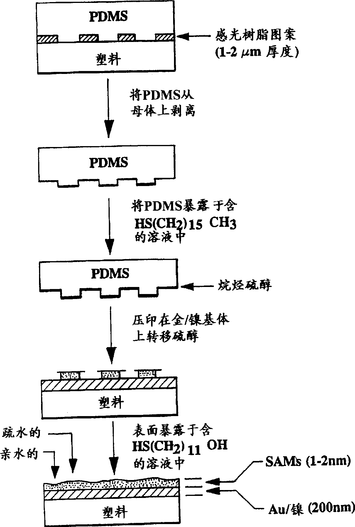
[0042] Gold-plated MYLAR(R) (polyethylene terephthalate) was printed with a pattern of 16-mercaptohexadecanic acid and cetylmercaptan.

[0043] Pattern printing of gold-plated MYLAR® (polyethylene terephthalate) with a pattern of 16-mercaptohexadecanic acid and cetyl mercaptan, such as figure 1 shown, and described below.

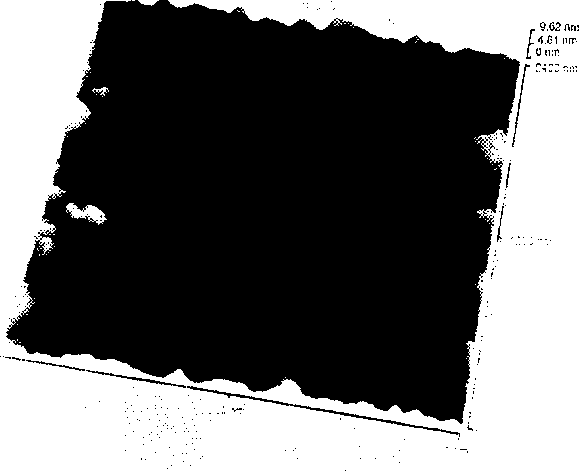
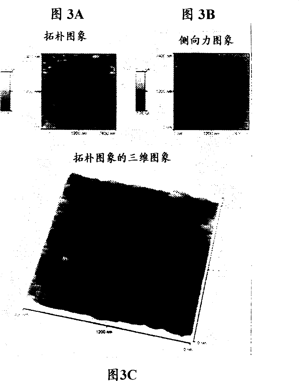
[0044] MYLAR(R) film modified with a plasma deposited gold topcoat was obtained from Courtaulds Performance Films (21034 Osborne Street, Canoga Park, CA 91304). figure 2 An atomic force microscope image of this MYLAR thin film is shown. A polymer film with a thickness of 2-7 mils and a gold overcoat that yields a surface resistance of 65 ohms per square centimeter and a visible light transmission of 20%-65% is used.

[0045] Hydrophilic carboxy-terminated alkanethiols were imprinted onto gold-coated films using 16-mercaptohexadecanoic acid by the following method. Light exposure of 10 micron diameter rings on a silicon wafer and the resulting photoresis...

Embodiment 2

[0048] Aluminum-coated MYLAR(R) was printed with 16-carboxyhexadecanoic acid and cetyl carboxylate.

[0049] With 1,16-hexadecane dihydroxamic acid and 1-hexadecane hydroxamic acid respectively replace the hydrophilic and hydrophobic mercaptan in embodiment 1, with 35% visible light transmittance to 100 standard Aluminum coated MYLAR(R) The method of Example 1 was followed. Diffraction of visible light. Reflection and transmission diffraction patterns can be observed when using 5mM, 670nM laser irradiation. Rainbow diffractive colors can be observed with transmitted white light. Example 3

Embodiment 3

[0050] The gold-coated MYLAR(R) was compared to a gold-coated silicon wafer.

[0051] Thin films of gold (100 angstroms to 1 micron) were deposited by electron beam evaporation on silicon wafers that had been pre-coated with titanium (5-50 angstroms) to promote adhesion between silicon and gold. Imprinting was performed as in Example 1 on gold-coated films and gold-coated silicon wafers.

[0052] Measurement of contact angle

[0053]The contact angle was measured with a Rame-Hart 100 goniometer at room temperature and ambient humidity. Water for contact angles was deionized and distilled in glass and taffeta apparatus. The advancing and receding contact angles of at least three drops of each liquid were measured on both sides of each slide, and the data in the figure represent the average of these measurements. Contact angles were measured using the following method: A drop with a volume of 1-2 microliters was formed on the end of a pipette (Micro-Electrapettesyringe, Matri...


PUM

PropertyMeasurementUnit
Thicknessaaaaaaaaaa

Abstract

The present invention comprises methods of contact printing of patterned, self-assembling monolayers of alkanethiolates, carboxylic acids, hydroxamic acids, and phosphonic acids on metallized thermoplastic films, the compositions produced thereby, and the use of these compositions. Patterned self-assembling monolayers allow for the controlled placement of fluids thereon which contain a chemically reactive, indicator functionality. The optical sensing devices produced thereby when the film is exposed to an analyte and light, can produce optical diffraction patterns which differ depending on the reaction of the self-assembling monolayer with the analyte of interest. The light can be in the visible spectrum, and be either reflected from the film, or transmitted through it, and the analyte can be any compound reacting with the fluid on the self-assembling monolayer. The present invention also provides a flexible support for a self-assembling monolayer on gold or another suitable metal.

Description

technical field [0001] The invention belongs to the field of contact printing, in particular, the invention belongs to microcontact printing on metal thin films such as gold. Background of the invention [0002] Microcontact printing is a technique for patterning organic monolayers with μm and submicron side dimensions. It has experimental simplicity and flexibility in forming certain types of patterns. It relies on the remarkable ability of self-integrated monolayers of long-chain alkane thiol salts to form on gold and other metals. These patterns can act as nanoprotective layers to protect the base metal from suitably formulated etchant, or they can allow selective placement of liquids in the hydrophilic regions of the patterns. Self-integrating monolayer patterns that can be smaller than 1 μm in size are formed by using alkanethiols as "inks" and printing them on metal substrates using elastic "stamps". The mold is made by molding a silicone elastomer from a matrix pre...

Claims


Application Information

Patent Timeline
IPC IPC(8): B05D1/28B41M3/00G03F7/00G03F7/16
CPCB82Y10/00G03F7/0002G03F7/161B41M3/003B82Y30/00B05D1/283B82Y40/00G03F7/165Y10T428/2804Y10T428/249983Y10T428/31703G03F7/028G03F7/033G03F7/0388G03F7/70958
Inventor D·S·埃维尔哈特G·M·惠特斯德斯
Owner KIMBERLY-CLARK WORLDWIDE INC
Why Eureka
Try Eureka