Method for manufacturing silicon high-speed semiconductor switch device

A technology of switching devices and manufacturing methods, which is applied in semiconductor/solid-state device manufacturing, electrical components, circuits, etc., can solve problems such as increased leakage current, poor reverse blocking characteristics, and decreased breakdown voltage, so as to improve switching speed , excellent electrical performance, and the effect of improving the softness factor

Inactive Publication Date: 2006-05-31
BEIJING UNIV OF TECH
View PDF2 Cites 0 Cited by
  • Summary
  • Abstract
  • Description
  • Claims
  • Application Information

AI Technical Summary

Problems solved by technology

[0003] The purpose of the present invention is to solve the above technical problems, and provide a method for manufacturing a silicon high-speed semiconductor switching device containing at least one pn junction, which can solve the poor reverse blocking characteristics (leakage current) of devices existing in the existing local lifetime control technology. increase and decrease in breakdown voltage), better exert the theoretical advantages of the concept of local lifetime control, and manufacture silicon semiconductor switching devices with better performance than the existing technology, which is manifested in faster switching speed and soft The degree factor is larger but has basically the same reverse blocking performance (I R and V on ); or have a lower I R and V on while having essentially the same switching speed and softness

Method used


Image

  • Method for manufacturing silicon high-speed semiconductor switch device
  • Method for manufacturing silicon high-speed semiconductor switch device
  • Method for manufacturing silicon high-speed semiconductor switch device

Examples


example 1

[0041] Example 1 Fast recovery pin diode manufacturing method:

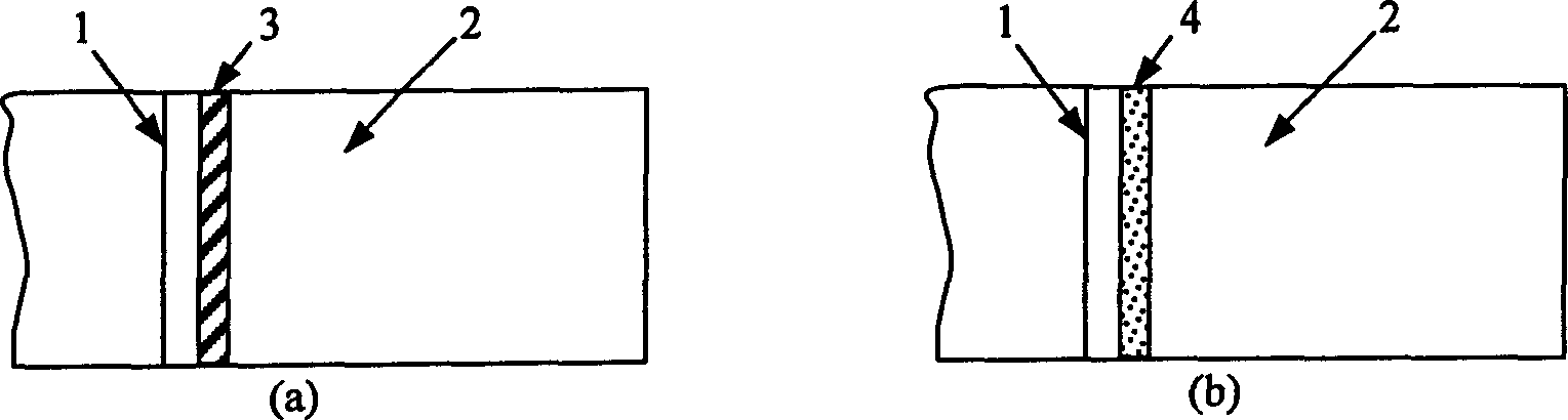
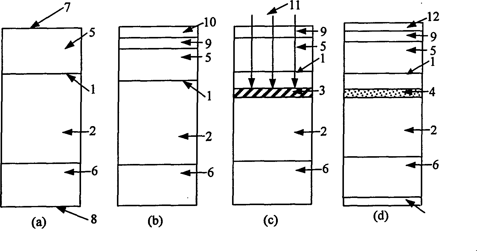
[0042] The step that the present invention manufactures pin fast recovery diode is, refer to attached figure 2 : (1) each p-type doping and n-type doping regions of the pin diode are produced by conventional methods, including a pn junction 1, a high-resistivity n-type base region 2, a low-resistivity p-type anode region 5, and a low-resistance n-type Cathode region 6, upper surface 7 and lower surface 8, see attached figure 2 (a). For epitaxial fast recovery diodes, the conventional method here is to epitaxially high-resistance n-type layer on a low-resistance n-type silicon substrate, and then diffuse p-type impurities from the surface into the high-resistance n-type layer; for double-diffused fast recovery diodes here The conventional method is to diffuse high-concentration n-type impurities and p-type impurities on both sides of the high-resistance n-type substrate; (2) remove the silicon dioxide on the s...

example 2

[0043] Example 2 Manufacturing method of high-speed insulated gate bipolar transistor (IGBT):

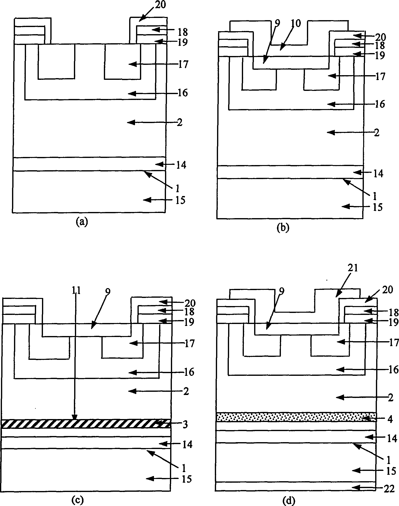
[0044] The step that the present invention manufactures high-speed IGBT is, referring to the attached image 3 : (1) The basic structures such as each p-type region and n-type region of the IGBT are manufactured by conventional methods, see the attached image 3 (a), it includes the p-type drain region 15 of low resistivity, the n-type base region 2 of high resistivity, the n-type buffer layer 14 of medium resistivity, pn junction 1, the p-type well region 16 of medium resistivity, low n-type source region 17 of resistivity, polysilicon gate electrode 18, gate oxide layer 19 etc.; Deposit a layer of platinum film with a thickness of about 0.1 to 0.2 microns; (3) place the silicon wafer in a heating furnace at a temperature of about 465° C. and keep it warm for about 40 minutes, so far a platinum-silicon alloy layer 9 is formed at the interface between platinum and silicon, leaving...


PUM

PropertyMeasurementUnit
thicknessaaaaaaaaaa

Abstract

The method is applicable to manufacture silicon semiconductor binistor with at least one PN junction such as GTO, IGBT etc. General manufacturing steps is carried out till the step of making metalized electrode. Platinum-silicon alloy is made on surface of silicon. Using proton orª‡particle injection forms local high density defect area. Heating and annealing makes the defect area absorb platinumto convert to platinum impurity range. Then, General manufacturing steps is carried out till manufacturing completion. The performances of the invention are better than present life control technique. The parts made by the invention possesses higher switching speed and backward recovery speed, but the forward voltage drop and reverse leakage are not increased visibly.

Description

Technical field: [0001] The invention relates to a manufacturing method of a silicon high-speed semiconductor switching device, which is suitable for manufacturing a silicon semiconductor switching device containing at least one pn junction, such as a fast recovery diode, a thyristor, a gate turn-off thyristor (GTO), an insulated gate bipolar Fabrication of transistors (IGBTs) and bipolar switching transistors. Background technique: [0002] In power electronic devices, such as switching power supplies, inverters, etc., various semiconductor switching devices are used. An important requirement for switching devices is that the power loss of the device is small. This requires a fast switching speed of the device (in the current recovery time t during the turn-off process r small to mark) to reduce switching loss, reverse leakage I R small to reduce off-state losses, the forward voltage drop V on small to reduce on-state losses. In addition, the fast recovery diode also r...

Claims


Application Information

Patent Timeline
Patent Type & Authority Patents(China)
IPC IPC(8): H01L21/322H01L21/265H01L21/328
Inventor 亢宝位贾云鹏
Owner BEIJING UNIV OF TECH
Why Eureka
Try Eureka