Preparation of Yb-Gd-Ga doped garnet planar optical waveguide

A planar optical waveguide and garnet technology, applied in the direction of optical waveguide and light guide, can solve the problem that GGG crystals are difficult to process micron-scale wafers, and achieve good economic benefits and material saving effects

Inactive Publication Date: 2007-04-04
SHANGHAI INST OF OPTICS & FINE MECHANICS CHINESE ACAD OF SCI
View PDF5 Cites 0 Cited by
  • Summary
  • Abstract
  • Description
  • Claims
  • Application Information

AI Technical Summary

Problems solved by technology

[0008] The technical problem to be solved in the present invention is to overcome the large block Yb grown in the prior art 3+ : The problem that GGG crystals are difficult to process into micron-scale wafers, and a preparation method of Yb-doped GdGa garnet planar optical waveguide is provided to meet the needs of the micro-optics field and the growing laser technology and integrated optics

Method used


Image

  • Preparation of Yb-Gd-Ga doped garnet planar optical waveguide

Examples


Embodiment 1

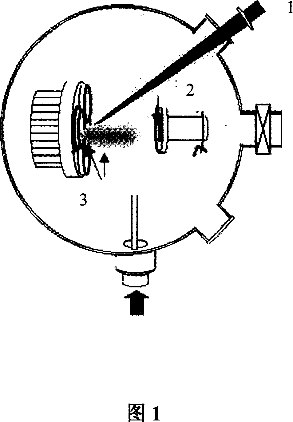
[0019] Yb was prepared by pulsed laser deposition (PLD) as described above 3+ :GGG single crystal thin film device and specific process flow:

[0020] The size to be cleaned is 10×10mm 2 , double-sided polished pure YAG substrate 2 and Yb 3+ : GGG polycrystalline target 3 is sent into the pulsed laser deposition system;

[0021] Evacuate the cavity into an ultra-high vacuum, and then fill it with an oxygen atmosphere;

[0022] Heating the substrate to 600°C, passing the ArF excimer laser 1 with a pulse width of 25ns through the lens at 10J / cm 2 The energy density of the concentrated light is irradiated to the Yb in the device through the optical window 3+ : GGG polycrystalline target 3, the surface molecules of the target 3 are melted and evaporated to form a film on the pure YAG substrate 2, and high-quality Yb can be obtained after slow cooling 3+ : GGG film.

Embodiment 2

[0024] Yb was prepared by pulsed laser deposition (PLD) as described above 3+ :GGG single crystal thin film device and specific process flow:

[0025] The size to be cleaned is 10×10mm 2 , double-sided polished pure YAG substrate and Yb 3+ : The GGG polycrystalline target is sent into the pulsed laser deposition system;

[0026] Evacuate the cavity into an ultra-high vacuum, and then fill it with an oxygen atmosphere;

[0027] Heating the substrate to 900°C, passing the ArF excimer laser with a pulse width of 25ns through the lens at 10J / cm 2 The energy density of the concentrated light is irradiated to the Yb in the device through the optical window 3+ : GGG polycrystalline target, the target surface molecules are melted and evaporated to form a film on a pure YAG substrate, and high-quality Yb can be obtained after slow cooling 3+ : GGG planar optical waveguide.

Embodiment 3

[0029] Yb was prepared by pulsed laser deposition (PLD) as described above 3+ :GGG single crystal thin film device and specific process flow:

[0030] The size to be cleaned is 10×10mm 2 , double-sided polished pure YAG substrate and Yb 3+ : The GGG polycrystalline target is sent into the pulsed laser deposition system;

[0031] Evacuate the cavity into an ultra-high vacuum, and then fill it with an oxygen atmosphere;

[0032] Heating the substrate to 800°C, passing the ArF excimer laser with a pulse width of 25ns through the lens at 10J / cm 2 The energy density of the concentrated light is irradiated to the Yb in the device through the optical window 3+ : GGG polycrystalline target, the target surface molecules are melted and evaporated to form a film on a pure YAG substrate, and high-quality Yb can be obtained after slow cooling 3+ : GGG planar optical waveguide.


PUM


Abstract

A method for preparing planar optical waveguide of garnet doped with Yb-Gd-Ga applies pulse laser depositing method to fuse out surface layer molecule of Yb3+: GGG multicrystal target material and to generate Yb3+:GGG planar optical waveguide on heated pure YAG substrate. A Yb3+: GGG planar optical waveguide on the requirement in micron grade cand be growed up by utilizing the method.

Description

technical field [0001] The invention relates to a planar optical waveguide, in particular to a method for preparing a planar optical waveguide doped with ytterbium-gadolinium-gallium garnet, in particular to growing a layer of Yb on a pure YAG single crystal substrate 3+ : GGG single crystal thin film, which is an excellent planar optical waveguide material. Yb 3+ : GGG planar optical waveguide is an excellent laser and optoelectronic material, and has a very wide application prospect. Background technique [0002] Yb 3+ Ions are the simplest active ions, with only one ground state and one excited state. Its advantages are: [0003] 1.Yb 3+ The ion absorption band is in the wavelength range of 0.9-1.1 μm, which can be coupled with the InGaAs laser diode pump source, and has an absorption bandwidth; [0004] 2. Low quantum defects; [0005] 3. There is no excited state absorption and upconversion, and the photoconversion efficiency is high; [0006] 4. The fluorescenc...

Claims


Application Information

Patent Timeline
Patent Type & Authority Patents(China)
IPC IPC(8): G02B6/13G02B6/10
Inventor 赵志伟姜本学徐军
Owner SHANGHAI INST OF OPTICS & FINE MECHANICS CHINESE ACAD OF SCI
Why Eureka
Try Eureka