Method of raising the field electron emitting performance of carbon nanotube film

A field electron emission, carbon nanotube thin film technology, applied in nanotechnology, nanotechnology, nanostructure manufacturing and other directions, can solve the problems of unfavorable large-area growth, high growth temperature, high cost, and improve field emission performance, reduce Threshold field strength, the effect of improving uniformity

Inactive Publication Date: 2002-05-15
SHANGHAI INST OF MICROSYSTEM & INFORMATION TECH CHINESE ACAD OF SCI
View PDF0 Cites 9 Cited by
  • Summary
  • Abstract
  • Description
  • Claims
  • Application Information

AI Technical Summary

Problems solved by technology

The CNTs grown by the direct growth method have good bonding force to the substrate and high purity, but the growth temperature is generally high, which

Method used


Image

  • Method of raising the field electron emitting performance of carbon nanotube film
  • Method of raising the field electron emitting performance of carbon nanotube film
  • Method of raising the field electron emitting performance of carbon nanotube film

Examples


Embodiment 1

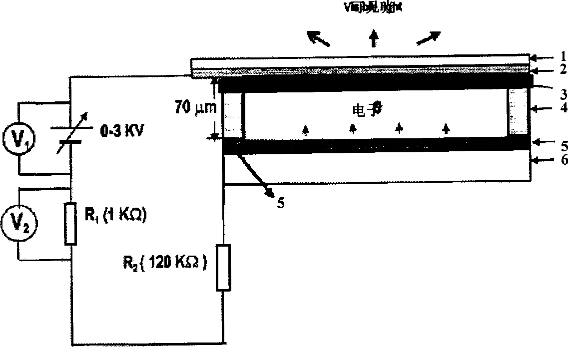
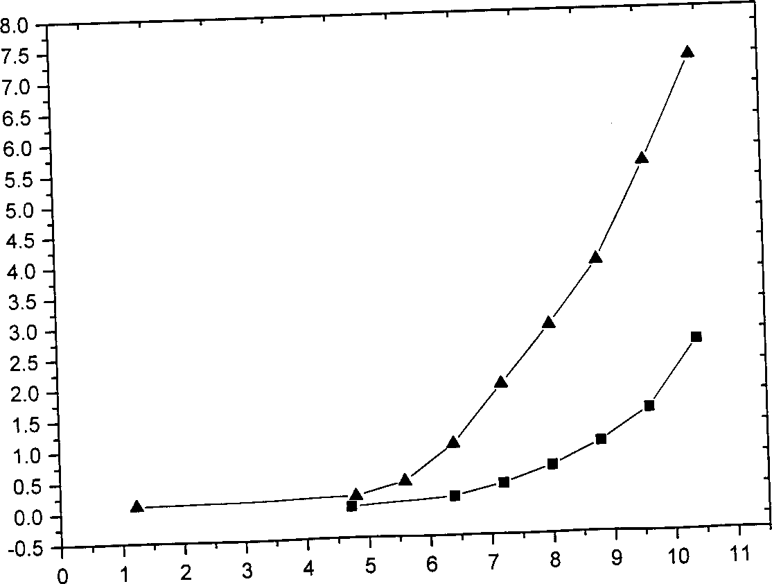
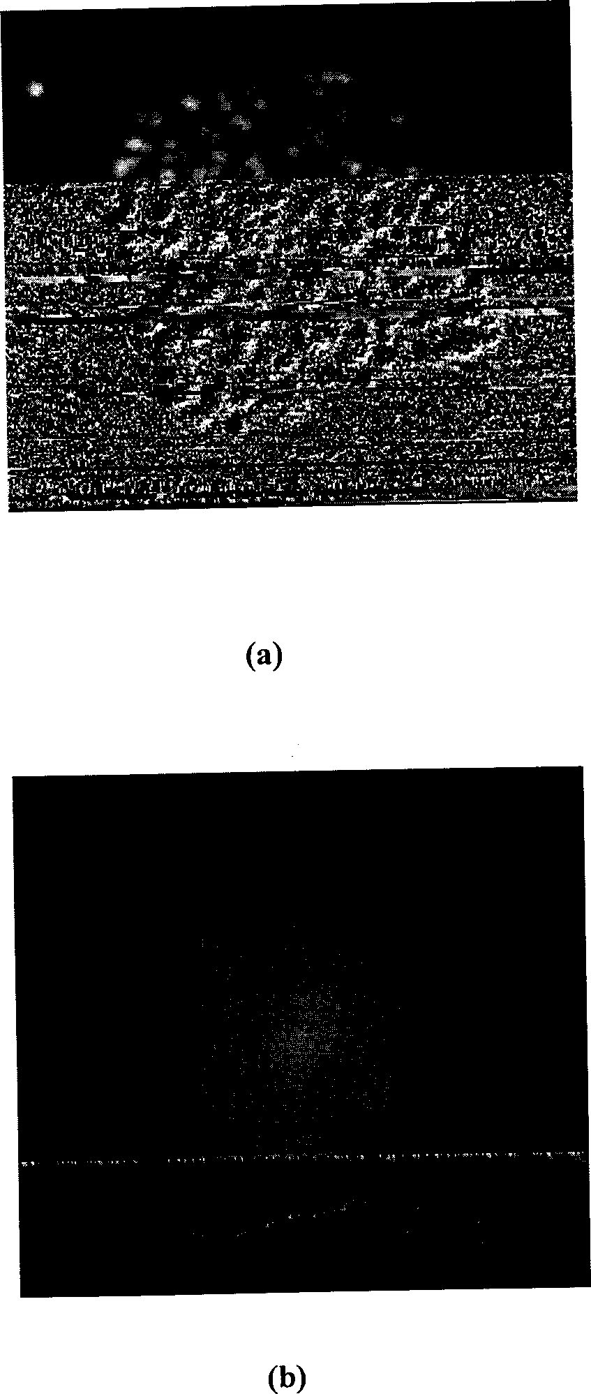
[0013] The field electron emission performance of the CNT thin film cathodes treated by the invention and not treated by the invention were tested. The CNT film cathode used is prepared by screen printing method, the substrate material is metallic nickel (Ni), the thickness of the CNT film is about 40 μm, and the effective area is 10 mm×10 mm. The tested samples are CNT films without any treatment and CNT films subjected to heat treatment and plasma surface treatment according to the method of the present invention. The heat treatment process condition that adopts in the present embodiment is 600 ℃; H 2 -N 2 shielding gas, H 2 The flow rate is 0.2 l / min, N 2 Flow rate of 2 l / min: treatment time 10 minutes. The plasma surface treatment equipment used in this embodiment is a capacitively coupled plasma etching equipment. The process conditions are: plasma power density 0.275W / cm 3 , plasma sheath voltage 215V; hydrogen flow, gas flow rate 20 ml / min; working pressure 0.4 To...

Embodiment 2

[0015] The field electron emission performance of the CNT thin film cathodes treated by the invention and not treated by the invention were tested. The CNT thin film cathode used is prepared by screen printing method. The substrate material is glass with a layer of metal Ti grown. The growth of metal Ti adopts electron beam evaporation method with a thickness of 500nm. The thickness of the CNT film is about 40μm and the effective area is 10mm. ×10mm. The tested samples are CNT films without any treatment and CNT films subjected to heat treatment and plasma surface treatment according to the method of the present invention. Processing condition is the same as embodiment 1. The treatment effect is similar to Example 1.

Embodiment 3

[0017] The field electron emission performance of the CNT thin film cathodes treated by the invention and not treated by the invention were tested. The CNT film cathode used is prepared by screen printing method, the substrate material is silicon wafer (Si), the thickness of the CNT film is about 60 μm, and the effective area is 10mm×10mm. The tested samples are CNT films without any treatment and CNT films subjected to heat treatment and plasma surface treatment according to the method of the present invention. The heat treatment process condition that adopts in the present embodiment is 550 ℃; O 2 -N 2 shielding gas, O 2 The flow rate is 0.1 l / min, N 2 The flow rate is 2 liters / minute; the processing time is 10 minutes. The plasma surface treatment equipment used in this embodiment is a capacitively coupled plasma etching equipment. The process conditions are: plasma power density 0.275W / cm 3 , plasma sheath voltage 215V; ammonia gas flow, gas flow rate 30 ml / min; work...


PUM

PropertyMeasurementUnit
Thicknessaaaaaaaaaa
Thicknessaaaaaaaaaa

Abstract

The characteristic is to use heat treating technology and plasma volume surface processing technology for CNT film cathode produced by transfer method and use plasma surface processing technology forthe CNT film cathode produced by direct growing method. The technology parameter of plasma surface process is power density 0.1 to 3 W/cubic m, the processing time is 5 to 6 minutes. H2 or hydrogen-containing compound is used. By processing according to the invention method, current density of CNT film can be increased three times, density of electric emitting point can be increased more than three times and the uniformity is increased obviously. The film cathode grown by transfer method is organic combined by two processing technologies to increase field emitting function of CNT film cathode.

Description

technical field [0001] The invention relates to a method for improving the field electron emission performance of a carbon nanotube (CNT) film, more precisely, the method of combining a heat treatment process and a plasma surface treatment process to make the field electron emission performance of a CNT film A way to significantly improve. It belongs to field emission display field. Background technique [0002] Field emission has become a very active field in recent years. It is agreed internationally that Field Emission Display (FED) has broad prospects and future in the flat panel display market. Compared with liquid crystal displays, the performance of field emission displays is comprehensively ahead, with the advantages of high brightness, better viewing angle effect, low power consumption, greatly reduced size, and simplified manufacturing process, etc., so it is known as the twenty-first A Century of Display Technology (K. Derbyshire, Solid State Technol. 38, 71 (1...

Claims


Application Information

Patent Timeline
IPC IPC(8): B82B3/00H01J1/304H01J9/02
CPCB82Y10/00H01J9/025
Inventor 冯涛王曦柳襄怀李琼
Owner SHANGHAI INST OF MICROSYSTEM & INFORMATION TECH CHINESE ACAD OF SCI
Why Eureka
Try Eureka