Direct writing of optical device in silica-based glass using femtosecond pulse lasers
A pulse and quartz technology, applied in the direction of optical components, laser welding equipment, laser components, etc., can solve the problems of repetition rate compromise
- Summary
- Abstract
- Description
- Claims
- Application Information
AI Technical Summary
Problems solved by technology
Method used
Image

Examples
example 1
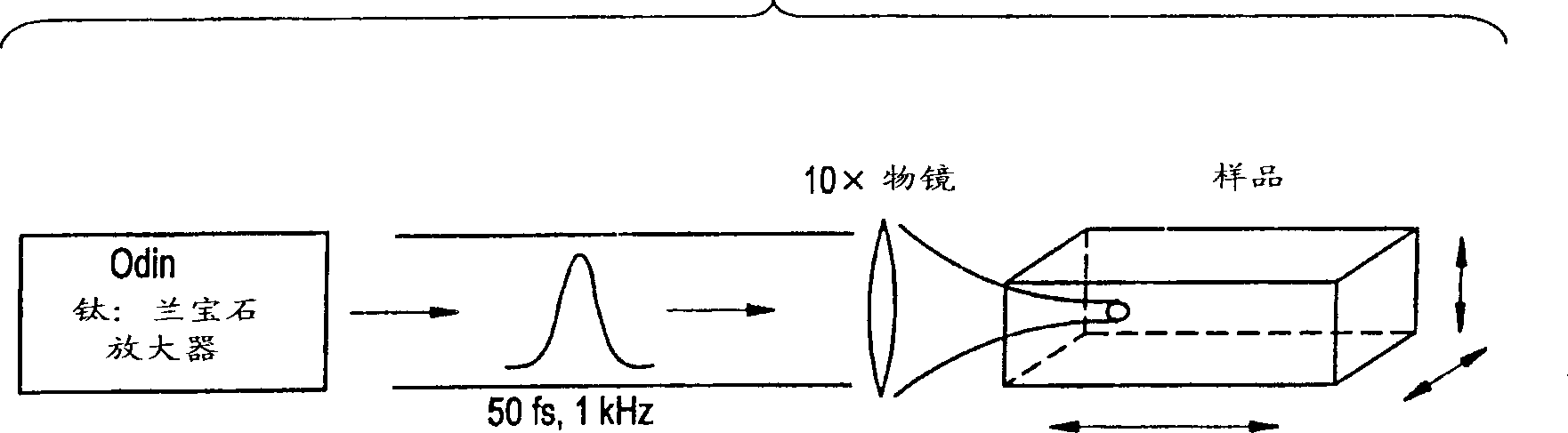
[0060] Using a 10× (0.16NA) clear mirror objective lens, the pulse from the titanium: sapphire multipass amplifier is focused into the fused silica glass sample. The duration of the pulse is 60fs, the pulse energy is about 1μJ, and the sample is mounted on a computer-controlled high-precision three-dimensional translation stage. The fused silica sample is translated through the beam focus at a rate of 30 μm / s, forming a waveguide structure in the bulk. Example 2
example 2
[0061] An 830nm laser is used to provide 40fs pulses with a repetition rate of 1kHz, and the unit pulse energy is about 1-5μJ. A lens with a numerical aperture of 0.16 in air is used to focus the beam into the glass below the surface. The sample is under the beam at about 5-100μm / s moving at a rate of . Keeping the experimental conditions unchanged, for fused silica and 14wt.%GeO 2 -86wt.% SiO 2 Sample exposure. The beam is focused approximately 1 μm below the glass surface. For samples irradiated under the same exposure conditions, the diameter of the germanium oxide-quartz sample affected by laser light is twice that of the fused silica sample. From this result, it was confirmed that the germania-quartz material is more sensitive than fused silica to changes in the refractive index caused by ultrafast laser exposure. Example 3
example 3
[0062]Axial scribing uses focused laser radiation to expose substrates of various glass compositions, i.e. SiO 2 (Corning product 7980) (22wt.%GeO 2 -78wt.% SiO 2 and 9 wt.% B 2 o 3 -91wt.% SiO 2 ). The laser wavelength is 830nm, the pulse duration is 40fs, the unit pulse energy is 1.0μJ, the repetition frequency is 1KHz, and the scanning speed is 20μm / s. After exposure, according to the far-field pattern generated by the waveguide, the refractive index change at 633nm was estimated, and the results are listed in Table 1. The annealing point for each material is also listed in Table 1.
[0063] Glass composition (% by weight)
[0064] Axial inscription with focused laser radiation on 9wt.% B 2 o 3 -91wt.% SiO 2 Exposure of glass samples. The laser wavelength is 830nm, the pulse duration is 40fs, the unit pulse energy is 1.0μJ, the repetition frequency is 1KHz, and the scan rate is 20μm / s. The far-field patterned micrograph of this sample is shown in Figu...
PUM
| Property | Measurement | Unit |
|---|---|---|
| Light intensity | aaaaa | aaaaa |
| Diameter | aaaaa | aaaaa |
| Line spacing | aaaaa | aaaaa |
Abstract
Description
Claims
Application Information
 - R&D
- Intellectual Property
- Life Sciences
- Materials
- Tech Scout
- Unparalleled Data Quality
- Higher Quality Content
- 60% Fewer Hallucinations
Browse by: Latest US Patents, China's latest patents, Technical Efficacy Thesaurus, Application Domain, Technology Topic, Popular Technical Reports.
© 2025 PatSnap. All rights reserved.Legal|Privacy policy|Modern Slavery Act Transparency Statement|Sitemap|About US| Contact US: help@patsnap.com