Preparation process of deep submicron integrated circuit Cu barrier

An integrated circuit, deep sub-micron technology, applied in the manufacturing of circuits, electrical components, semiconductor/solid-state devices, etc., can solve the problems of poor film uniformity, asymmetric thickness of sidewall step coverage, etc., to improve hole filling and thickness uniformity. The effect of improving the resistance to Cu diffusion and improving the ability to resist F diffusion

Inactive Publication Date: 2003-04-30
SHANGHAI HUA HONG GROUP +1
View PDF0 Cites 2 Cited by
  • Summary
  • Abstract
  • Description
  • Claims
  • Application Information

AI Technical Summary

Problems solved by technology

The limitation of long-range physical deposition is that the uniformity of the film is poor, and due to the influence of the shadow effect, the thickness of the sidewall step coverage in the pattern near the edge area of ​​the silicon wafer is asymmetric

Method used


Image

  • Preparation process of deep submicron integrated circuit Cu barrier

Examples


Embodiment Construction

[0024] Below further describe the present invention by specific embodiment:

[0025] 1. Using multi-chamber ion physical deposition (IPVD) equipment, degas the silicon wafer under low vacuum conditions at a temperature of 350°C for 180 seconds to eliminate water vapor and other impurities on the surface;

[0026] 2. Use Ar 2 and H 2 The plasma pre-treats the surface of the silicon wafer to remove the natural oxide layer in the through hole and the residue left by the previous process. The preprocessing time is 20 seconds;

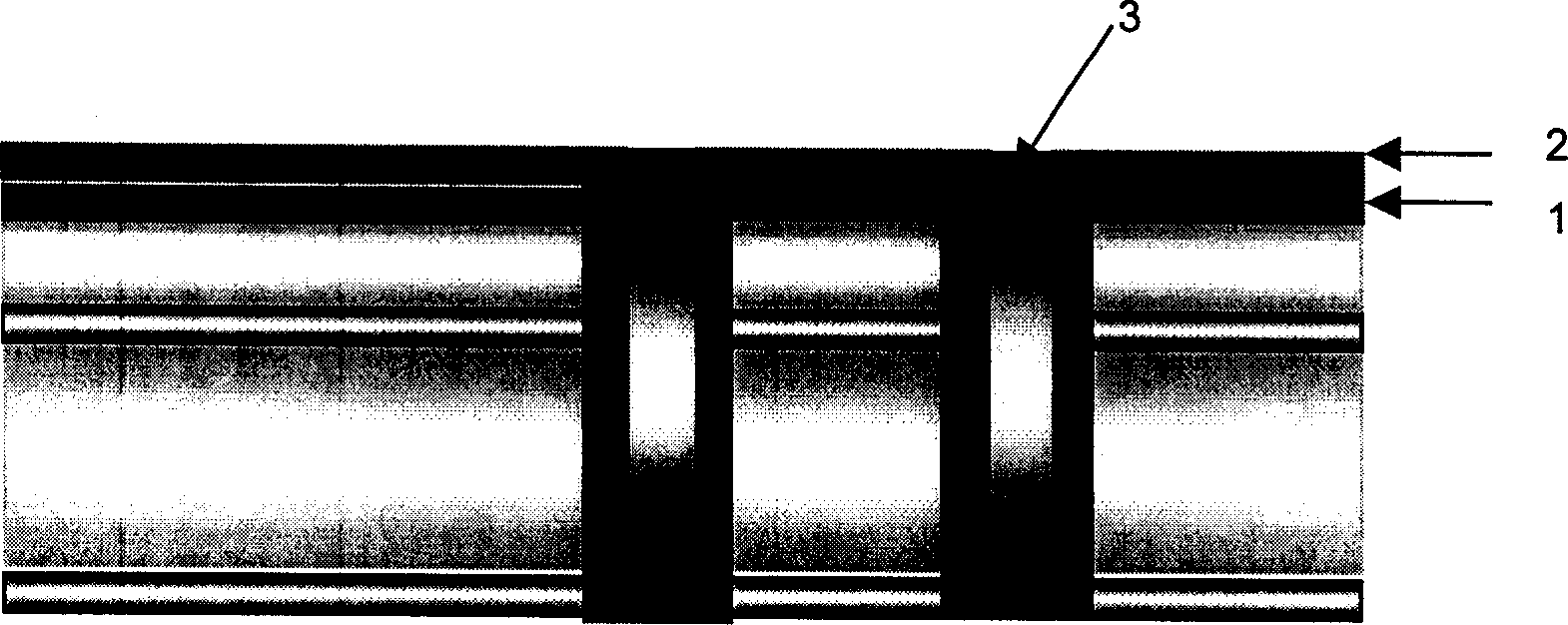
[0027] 3. Deposit a TaSiN barrier layer with a thickness of 30 nm by ion physics (IPVD) method;

[0028] 4. Deposit Ta on TaSiN by ion physics (IPVD) method, with a thickness of 20nm;

[0029] 5. Next, deposit a Cu seed layer with a thickness of 200nm by ion physics (IPVD) method;

[0030] 6. The silicon wafer with ion physical (IPVD) deposited Cu seed layer is sent into the Cu electroless plating tank, and a 1000nm Cu metal thin film is electroplated....


PUM

PropertyMeasurementUnit
thicknessaaaaaaaaaa
thicknessaaaaaaaaaa
thicknessaaaaaaaaaa

Abstract

A preparing process for Cu blocking layer of integrated circuit in deep submicron uses the IPVD process to deposite TaSiN as a blocking layer to Cu diffusing and to select Ta as an adjacent blocking layer material of Cu metal. In chemical electroplating of Cu, the alternating electric field and electroplating additives are applied. The heat treatment for Cu with annealing in fast heating and the chemicomechanical polishing for Cu is carried out to grind off the unnecessary Cu metal and blocking layer in addition to connection wire and through hole to realize the Cu interconnection wiring technology of Damascus. The process raises the ability of antidiffusing for Cu and F, improves the sticking ability with Cu metal film and insulation media, is suitable to be used in the interconnection technology of Cu metal and low dielectric material.

Description

technical field [0001] The invention belongs to the technical field of semiconductor integrated circuit manufacturing technology, and in particular relates to a preparation technology of a deep submicron integrated circuit Cu barrier layer. Background technique [0002] With the continuous reduction of integrated circuit design rules, the line width of the feature size has been reduced to 0.10 microns, and the trend of continuous downward reduction is maintained. On the other hand, the density of devices in integrated circuits continues to increase, the number of metal wiring layers is increasing, and the number of wiring layers in logic circuits has reached 7-8 layers. Due to the increase of the resistance of the metal interconnection line itself and its parasitic capacitance, the resulting RC interconnection delay has greatly surpassed the gate delay of the transistor itself, and has become a limiting factor for the speed of the integrated circuit. [0003] At present, th...

Claims


Application Information

Patent Timeline
Patent Type & Authority Applications(China)
IPC IPC(8): H01L21/283H01L21/3205H01L21/768
Inventor 徐小诚缪炳有
Owner SHANGHAI HUA HONG GROUP
Why Eureka
Try Eureka