Radiator and semiconductor element using such radiator and semiconductor packing body

A technology for semiconductors and radiators, applied in semiconductor devices, semiconductor/solid-state device components, electrical components, etc., can solve the problems of suppressing the processing speed, output and integration of semiconductor components, and achieve good airtightness and sealing, Less occurrence of thermal stress and high reliability

Inactive Publication Date: 2004-05-26
KOBE STEEL LTD
View PDF2 Cites 15 Cited by
  • Summary
  • Abstract
  • Description
  • Claims
  • Application Information

AI Technical Summary

Problems solved by technology

[0007] The heat dissipation characteristics of these existing heat sinks and semiconductor packages using the heat sink have been improved to the limit in terms of materials and structures, and it has been considered that it is very difficult to improve the heat dissipation characteristics. The current situation This is the case, in order to suppress the temperature rise of the package, the processing speed, output and integration of semiconductor elements have to be suppressed

Method used


Image

  • Radiator and semiconductor element using such radiator and semiconductor packing body
  • Radiator and semiconductor element using such radiator and semiconductor packing body
  • Radiator and semiconductor element using such radiator and semiconductor packing body

Examples


Embodiment 1

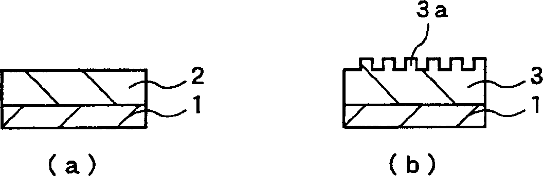
[0073] A diamond layer with a thermal conductivity of 800 W / m·K or higher was formed on the back surface of the silicon wafer by CVD (Chemical Vapor Growth). Diamond is microcrystalline with a thickness of 0.05 mm. In order to suppress warpage of the wafer and facilitate separation into individual chips, notches are formed on the wafer in advance to make the diamond layer a discontinuous film. Using such a silicon wafer, a semiconductor element was produced on the surface opposite to the surface on which the diamond was formed, and a semiconductor element and a module chip with an outer shape of 23 mm x 25 mm with a diamond heat sink were fabricated. The power consumption is 70W.

Embodiment 2

[0075] The semiconductor chip of Example 1 was fabricated using such a flip-chip semiconductor package as a package for mounting a 478-pin semiconductor element. As a resin wiring base material, a liquid crystal polymer is used as a main ingredient, and copper foil is thermocompressed on both sides. Copper foil is etched and patterned to form a wiring layer, and an insulating resin is covered thereon. The other copper foil was left as it is. Chips are mounted by wire bonding to form a semiconductor package.

[0076] In addition, the semiconductor element and module with a heat sink layer of the present invention are not limited to BGA semiconductor packages, and can be applied in various forms.

Embodiment 3

[0078] An aluminum heat sink with an outer shape of 35 mm×39 mm was attached to the semiconductor package of the second embodiment. Ten samples of two types were prepared. One sample covered a part of the surface of the diamond heat sink with aluminum with a thickness of 100nm, and the other sample coated the surface of the heat sink and ciliated diamond. Samples of polymer adhesives were tested for thermal cycling. In the test, -40°C / room temperature / 110°C was defined as one cycle, and 500 cycles were performed. In each example, 10 samples were tested, and the occurrence of cracks between the aluminum heat sink and the aluminum heat sink was examined, but no abnormality was observed.


PUM

PropertyMeasurementUnit
thermal conductivityaaaaaaaaaa
thicknessaaaaaaaaaa
thicknessaaaaaaaaaa

Abstract

A semiconductor device and package has a heat spreader directly disposed on the reverse surface of the semiconductor device. This heat spreader includes a diamond layer or a layer containing diamond and ceramics such as silicon carbide and aluminum nitride. The heat spreader is directly formed on a substrate for the semiconductor device. In particular, the heat spreader is composed of a diamond layer and one or two metal or ceramic members, which are bonded to the diamond layer with one or two polymer adhesive layers. This diamond layer has a fiber structure across the thickness or a microcrystalline structure. Cilia are formed on a surface of the diamond layer facing the one or two metal or ceramic members.

Description

technical field [0001] The present invention relates to a heat sink bonded to a semiconductor element in order to prevent a temperature rise caused by heat generated by the semiconductor element. Furthermore, the present invention relates to a semiconductor element and a semiconductor package with a heat sink. Background technique [0002] In order to cope with the improvement of heat dissipation of semiconductor elements, for example, a semiconductor package using a combination of a highly thermally conductive ceramic base material and a resin wiring board such as a printed circuit board has been proposed (JP-A-10-275879). In this semiconductor package, a heat sink made of aluminum nitride is used, and a semiconductor element is mounted on the lower side thereof, and a resin wiring board is bonded around the heat sink, and the signal wiring of the semiconductor element is surrounded by a wiring layer of the resin wiring board. Such a semiconductor package is expected to be...

Claims


Application Information

Patent Timeline
Patent Type & Authority Applications(China)
IPC IPC(8): H01L23/373
CPCH01L23/3732H01L2924/0002H01L2924/12044
Inventor 橘武史林和志井上宪一横田嘉宏小桥宏司川上信之古保里隆
Owner KOBE STEEL LTD
Why Eureka
Try Eureka