Supercharge Your Innovation With Domain-Expert AI Agents!

Formation of cobalt silicide film and manufacture of semiconductor device therewith

A cobalt silicide film, semiconductor technology, used in semiconductor/solid-state device manufacturing, semiconductor devices, transistors, etc.

Inactive Publication Date: 2004-07-07
SAMSUNG ELECTRONICS CO LTD
View PDF3 Cites 2 Cited by
  • Summary
  • Abstract
  • Description
  • Claims
  • Application Information

AI Technical Summary

Problems solved by technology

This brings limitations in reducing the aspect ratio of the gate 5b pattern, which adversely affects the process tolerance of subsequent processes

Method used


Image

  • Formation of cobalt silicide film and manufacture of semiconductor device therewith
  • Formation of cobalt silicide film and manufacture of semiconductor device therewith
  • Formation of cobalt silicide film and manufacture of semiconductor device therewith

Examples


no. 1 example

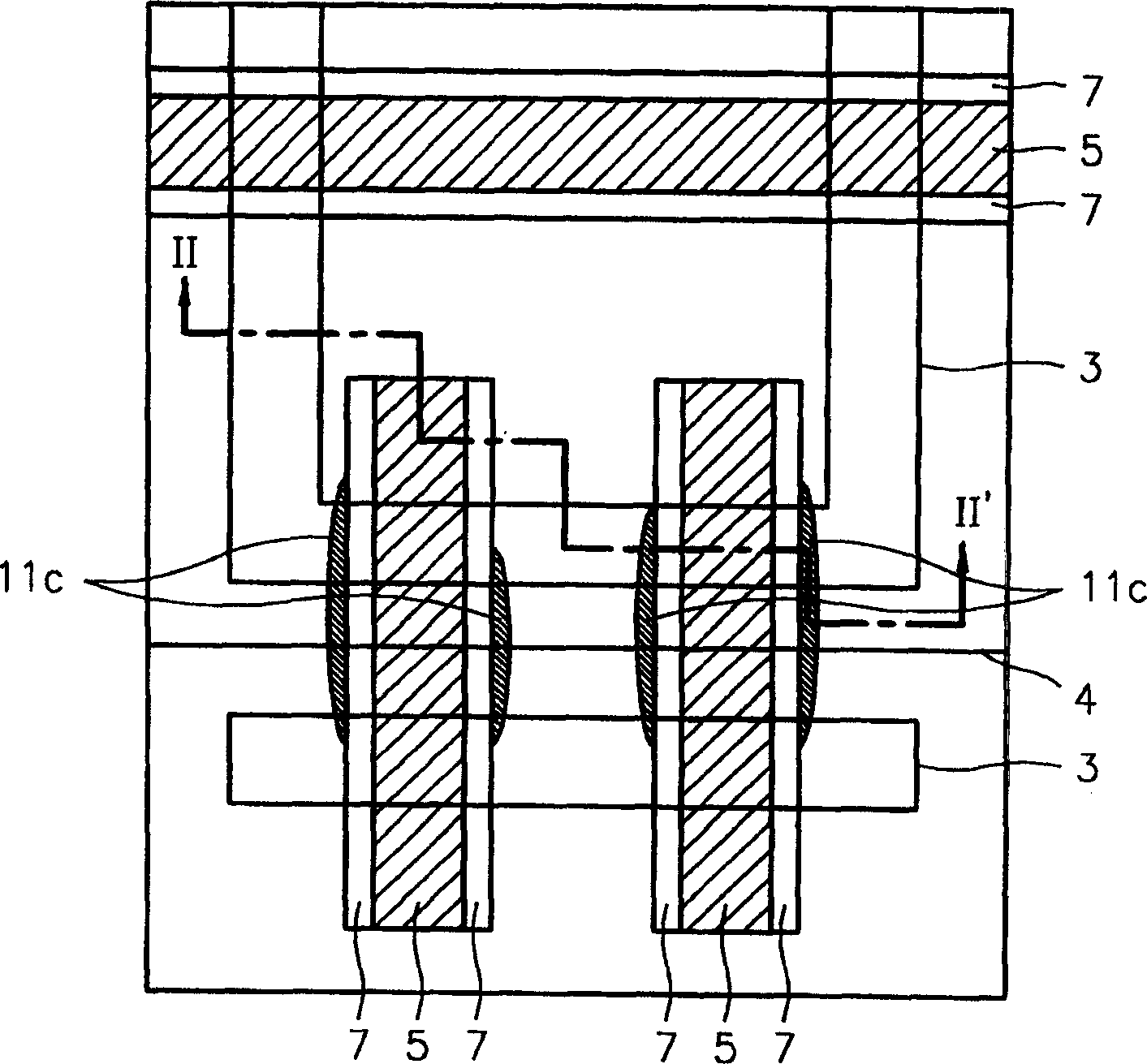
[0069] Using the following method for forming a cobalt silicide film according to the present invention, a 6-transistor (6Tr) SRAM cell was fabricated on a semiconductor wafer substrate according to a design standard of 110 nm, thereby preparing a test sample.

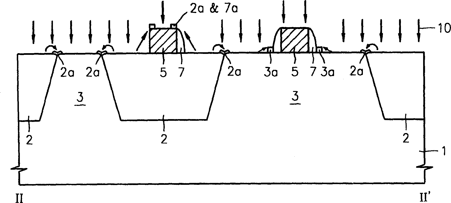
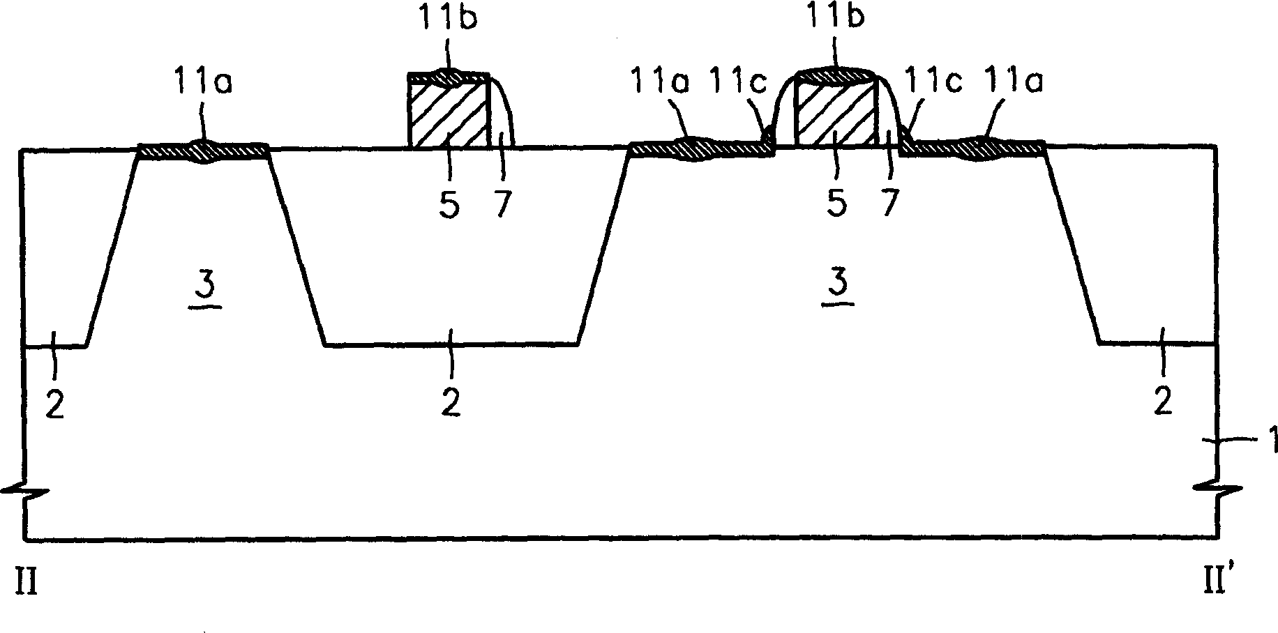
[0070] The front surface of the substrate with sidewall spacers and source / drain regions (hereinafter, referred to as "substructure") having a polysilicon gate pattern was wet-cleaned by using an SC1 solution followed by an HF solution. The substrate was etched by RF sputtering using argon (Ar) gas to remove the oxide film to a thickness of 50 Å, a cobalt film was formed by sputtering to a thickness of 100 Å, and was rich in titanium under a certain nitrogen flow rate. The titanium nitride covering film was formed to a thickness of 100 Å. RF sputter etching, cobalt film formation, and titanium nitride capping film formation are all performed in situ. According to Rutherford backscattering spectroscopy (RBS) analysis, ...

no. 2 example

[0077] The sheet resistance (Rs) of the NMOS grid and the PMOS grid in the test sample prepared in the first embodiment and the control sample were tested, and the results were as follows Figure 10A and 10B shown. Figure 10A Rs for the NMOS gate is shown, Figure 10B Rs for the PMOS gate is shown. exist Figure 10A and Figure 10B Middle: -○-represents the test sample, -□-represents the control sample.

[0078] Such as Figure 10A and Figure 10B As shown, while the test samples exhibited a very low and uniform Rs distribution, the control samples exhibited a high and inconsistent Rs distribution. This result indicates that the titanium-rich capping film effectively removes impurities such as oxides and nitrides existing in the interface between the cobalt film and the source / drain region or gate.

no. 3 example

[0080] Test samples and control samples were prepared in the same manner as in the first example. Secondary ion mass spectroscopy (SIMS) after primary RTA and after selective wet etching are shown in Figure 11A and 11B.

[0081] exist Figure 11A In and 11B: -◆- and -- represent test samples, -○- and -□- represent control samples. As shown in Figure 11B, the surface of the test sample (using a titanium-rich covering film) has a higher titanium content than the surface of the control sample (using a nitrogen-rich covering film), up to 10 2 times. In FIG. 11B , the region with a depth of 0 μm corresponds to the surface of the silicon region before the primary RTA, and at the same time, corresponds to the interface of the cobalt film and the cobalt silicide film before the selective wet etching. Judging from the fact that the silicon region is converted into a cobalt silicide film when cobalt diffuses toward the silicon region and the results of FIG. Impurities at the inte...


PUM


Abstract

A cobalt-containing film on a silicon-containing conductive region, and a titanium-rich capping layer is formed on cobalt-containing film. The atomic % ratio of titanium to other elements (if any) in the titanium-rich capping layer is more than one (1). The resultant structure is annealed so that cobalt of the cobalt-containing film and silicon of the silicon-containing conductive region react with each other to form a cobalt silicide film. When the formation of the cobalt-containing film is carried out at a high temperature, a diffusion restraint interface film is also formed.

Description

[0001] This is a continuation-in-part of US Patent Application Serial No. 10 / 457,449, filed June 10, 2003, which is incorporated herein by reference in its entirety. In addition, priority is claimed to Korean Patent Applications Nos. 2002-63567 and 2003-66498 with filing dates of October 17, 2002 and September 25, 2003, respectively, the entire contents of which are hereby incorporated by reference . technical field [0002] The present invention mainly relates to the manufacture of semiconductor devices, and more precisely, the present invention relates to a method of forming a cobalt silicide film and a method of manufacturing a semiconductor device having a cobalt silicide film. Background technique [0003] As the gate resistance and source / drain contact resistance of Metal Oxide Semiconductor (MOS) increase, the operating speed of semiconductor devices including MOS transistors decreases. Therefore, silicide films are widely used to reduce these resistances. Cobalt si...

Claims


Application Information

Patent Timeline
IPC IPC(8): C23C14/02C23C14/16C23C14/58H01L21/28H01L21/285H01L21/336H01L21/8238H01L21/8242H01L21/8244H01L21/8247H01L27/092H01L27/108H01L27/11H01L27/115H01L29/417H01L29/423H01L29/49H01L29/78
CPCH01L21/28518C23C14/165C23C14/5806C23C14/5873H01L29/665H01L21/28052C23C14/021
Inventor 具景谟具滋钦朴惠贞
Owner SAMSUNG ELECTRONICS CO LTD
Features
  • R&D
  • Intellectual Property
  • Life Sciences
  • Materials
  • Tech Scout
  • Unparalleled Data Quality
  • Higher Quality Content
  • 60% Fewer Hallucinations
Learn More