
Method for making polysilicon film

A technology of polysilicon thin film and manufacturing method, which is applied in semiconductor/solid-state device manufacturing, optics, instruments, etc., can solve problems such as inconsistency in grain size, poor uniformity of polysilicon thin film, and difficult control of excimer laser energy density, etc., to achieve The effect of good surface flatness

Inactive Publication Date: 2005-01-19
AU OPTRONICS CORP
View PDF0 Cites 7 Cited by
  • Summary
  • Abstract
  • Description
  • Claims
  • Application Information

AI Technical Summary

Problems solved by technology

[0008] Generally, in the crystallization process of the known polysilicon film, the energy density of the excimer laser must be controlled so that the amorphous silicon layer is almost completely melted, and at the same time, some unmelted amorphous silicon particles can be left as crystal seeds for crystallization. , so that there will be a better crystallization effect, but the excimer laser is a pulsed laser, and the energy density of each pulse will be different, so the control of the energy density of the excimer laser is not easy, so that the final grain size The size is inconsistent, and many protrusions (Protrusion) are formed at the grain boundary, which leads to poor uniformity of the polysilicon film and affects the device characteristics of the subsequent thin film transistor

Method used


Image

  • Method for making polysilicon film
  • Method for making polysilicon film
  • Method for making polysilicon film

Examples


no. 1 example

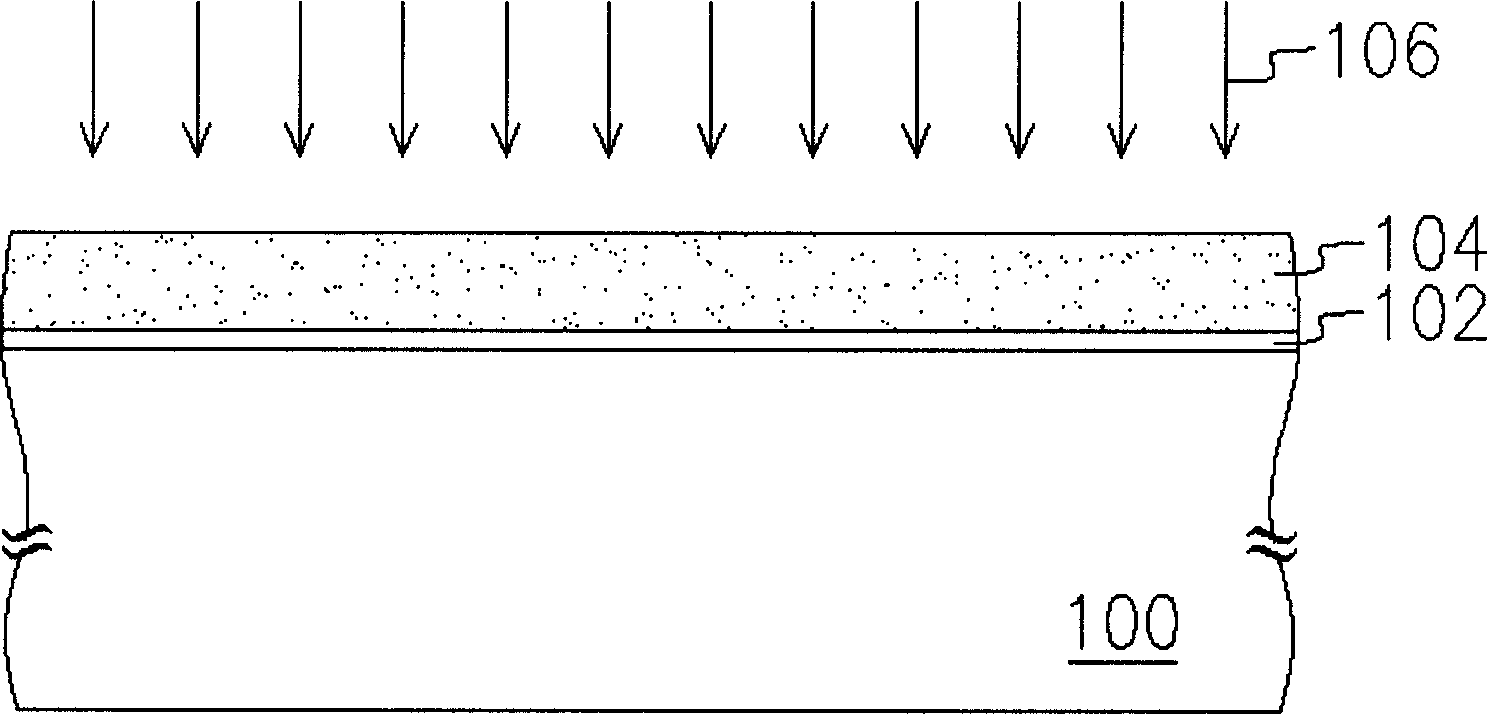
[0034] Please refer to Figure 2A to Figure 2F , which is a cross-sectional view of the manufacturing process of the polysilicon thin film according to the first embodiment of the present invention.

[0035] First, please refer to Figure 2A , providing a substrate 200, such as a silicon wafer, a glass substrate or a plastic substrate, forming an insulating layer 202 on the substrate 200, the material of the insulating layer 202 is, for example, silicon dioxide, and the formation method is, for example, A silicon dioxide layer is formed on the substrate 200 by Low Pressure Chemical Vapor Deposition (LPCVD), Plasma Enhanced Chemical Vapor Deposition (PECVD) or sputtering (Sputter) . Next, a layer of amorphous silicon layer 204 is formed on the insulating layer 202. The amorphous silicon layer 204 is formed by, for example, low pressure chemical vapor deposition, plasma enhanced chemical vapor deposition or sputtering, wherein the formed The amorphous silicon layer 204 has a ...

no. 2 example

[0045] Please refer to Figure 3A to Figure 3G , which is a cross-sectional view of the manufacturing process of the polysilicon thin film according to the second embodiment of the present invention.

[0046] First, please refer to Figure 3A , providing a substrate 300, such as a silicon wafer, a glass substrate or a plastic substrate, forming an insulating layer 302 on the substrate 300, wherein the material of the insulating layer 302 is, for example, silicon dioxide, and the forming method is, for example, A silicon dioxide layer is formed on the substrate 300 by low pressure chemical vapor deposition, plasma enhanced chemical vapor deposition or sputtering. Next, a layer of amorphous silicon layer 304 is formed on the insulating layer 302. The amorphous silicon layer 304 is formed by, for example, low-pressure chemical vapor deposition, plasma-enhanced chemical vapor deposition, or sputtering, wherein the formed The amorphous silicon layer 304 has a thickness D4, and th...


PUM

PropertyMeasurementUnit
Thicknessaaaaaaaaaa

Abstract

The invention provides a polycrystalline silicon film making method, using the phenomenon that as an ordinary polycrystalline silicon layer is formed, its surface saliences have different heights, and using partiall higher saliences to generate crystal seeds used in the following crystallizing step, therefore able to make the new formed polycrystalline silicon film have uniform and bigger crystal particles and have fewer lower-density saliences, and further have better surface flatness.

Description

technical field [0001] The invention relates to a manufacturing method of a thin film transistor liquid crystal display (TFT-LCD), and in particular to a manufacturing method of a polysilicon thin film of a thin film transistor array in the thin film transistor liquid crystal display. Background technique [0002] Generally, active array liquid crystal displays can be divided into polysilicon thin film transistors and amorphous silicon thin film transistors due to their materials. Polysilicon thin film transistors can provide higher aperture ratios and lower costs than amorphous silicon thin film transistors because they can integrate driving circuits. However, another reason why polysilicon thin film transistor technology is highly praised is that polysilicon thin film transistors can greatly reduce the size of components to achieve high resolution. Generally, polysilicon thin film transistor liquid crystal displays must have low-temperature manufacturing technology (about 4...

Claims


Application Information

Patent Timeline
IPC IPC(8): G02F1/136H01L21/00H01L21/20
Inventor 张茂益
Owner AU OPTRONICS CORP
Learn More