Process for preparing vanadium oxide film capable of regulating phase change temp.
A vanadium oxide film, phase transition temperature technology, applied in metal material coating process, vacuum evaporation coating, coating and other directions, can solve the problems of high phase transition temperature, changing stress level, affecting stability, etc., to achieve infrared transmission. High pass rate, small package size, and the effect of improving the response rate
- Summary
- Abstract
- Description
- Claims
- Application Information
AI Technical Summary
Problems solved by technology
Method used
Image
Examples
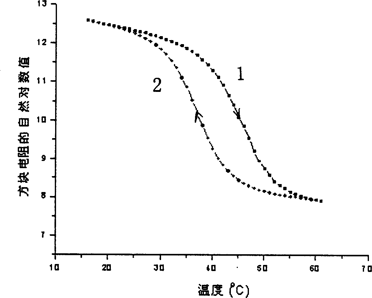
Embodiment 1
[0023] Embodiment 1 Phase transition temperature is the preparation method of vanadium oxide thin film of 28 ℃, comprises the following steps successively:
[0024] (1) The silicon wafer is cleaned by standard RCA to remove the polluting organic matter, dust and metal ion impurities on the surface of the silicon wafer. The ion beam sputtering method is used to deposit a layer of silicon oxide film on the silicon wafer. The target material used is SiO2 target material, the background vacuum is 3×10 -3 Pa, through argon to 2.6×10 -2 Pa, the ion beam power is 25W, the sputtering time is 20 minutes, the film thickness is about 50 nanometers, and then a layer of silicon nitride film is deposited. The target material used is silicon nitride target material, and the background vacuum is 2.4×10 -3 Pa, through argon to 2.6×10 -2 Pa, the ion beam power is 25W, the sputtering time is 45 minutes, and the film thickness is about 100 nanometers.
[0025] The above-mentioned silicon oxide...
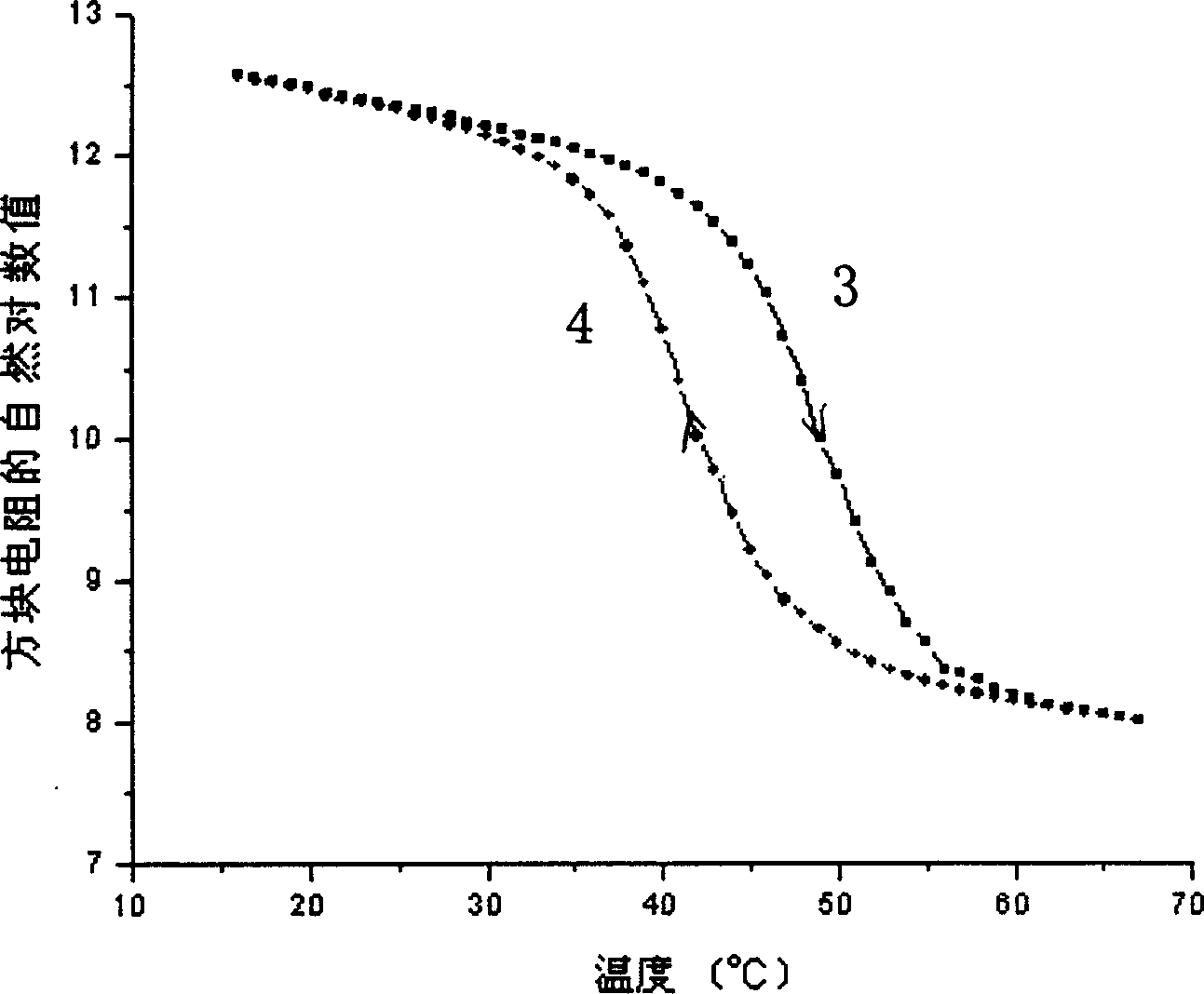
Embodiment 2
[0029] Example 2 The method for preparing a vanadium oxide thin film with a phase transition temperature of 39°C includes the following steps in sequence:
[0030] (1) The silicon wafer is cleaned by standard RCA to remove the polluting organic matter, dust and metal ion impurities on the surface of the silicon wafer. Using the ion beam sputtering method, a layer of silicon oxide film is first deposited on the silicon wafer. The film thickness is about 100 nanometers, and then deposit a layer of silicon nitride film, the film thickness of which is about 50 nanometers.
[0031] (2) The vanadium oxide film is deposited on the above-mentioned silicon nitride film by ion beam reactive sputtering method, and the ion beam reactive sputtering process condition is: background vacuum 9×10 -4 Pa, through oxygen and argon, oxygen pressure 1×10 -3 Pa, argon pressure 1.5×10 -2 Pa, the ion beam current power is 25W, the substrate temperature is 350°C, and the sputtering time is 25 minutes...
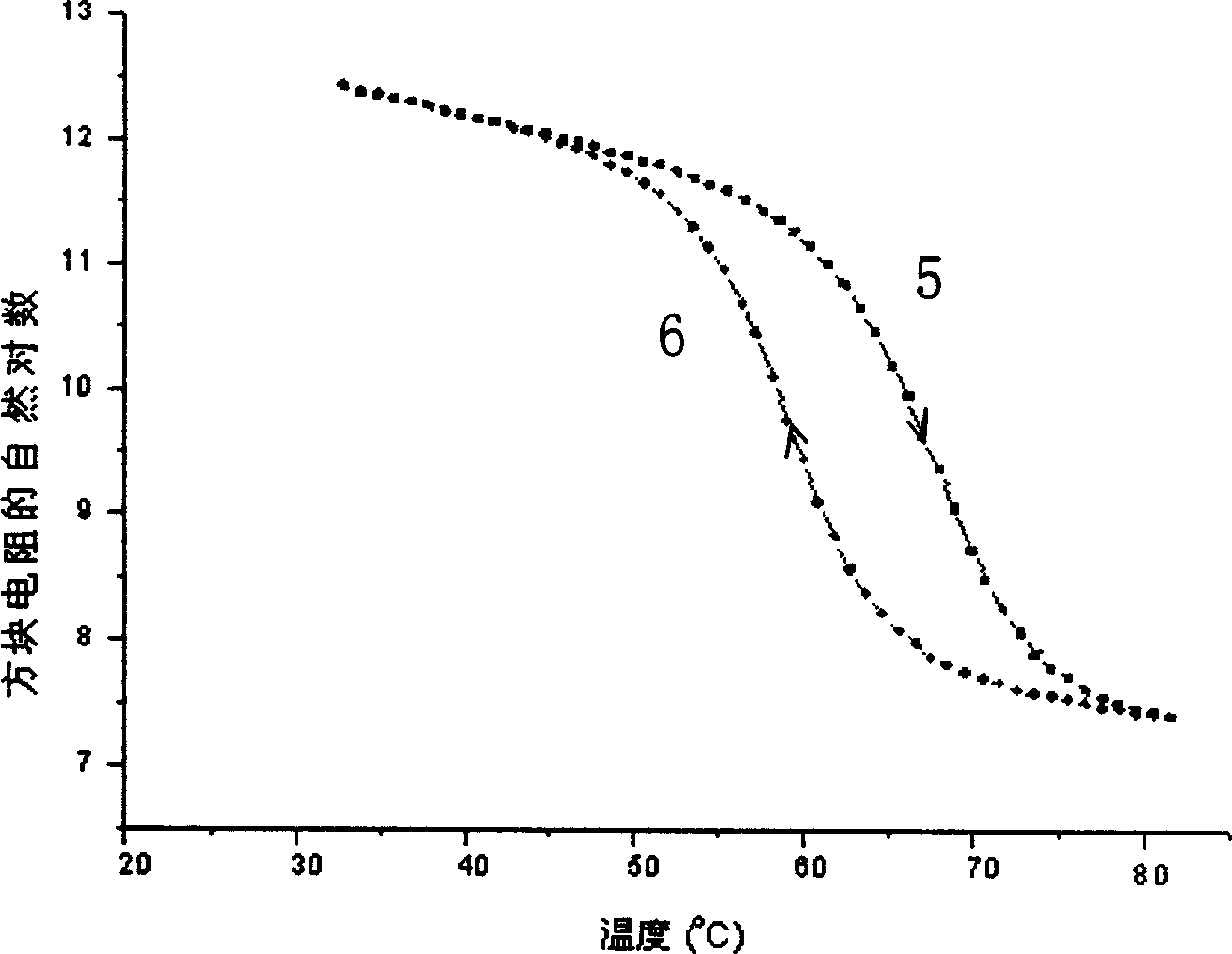
Embodiment 3
[0034] Example 3 The phase transition temperature is a method for preparing a vanadium oxide thin film of 57°C, which includes the following steps in turn:
[0035](1) The silicon wafer is cleaned by standard RCA to remove the polluting organic matter, dust and metal ion impurities on the surface of the silicon wafer. Using the ion beam sputtering method, a layer of silicon oxide film is first deposited on the silicon wafer. The film thickness is about 70 nanometers, and then deposit a layer of silicon nitride film, the film thickness of which is about 85 nanometers.
[0036] (2) Using the ion beam reactive sputtering method, the vanadium oxide film is deposited on the above-mentioned silicon nitride film, and the ion beam reactive sputtering process conditions are: the background vacuum is 1.6×10 -3 Pa, through oxygen and argon, oxygen pressure 6.1×10 -3 Pa, argon pressure 1.8×10 -2 Pa, the ion beam current power is 45W, the substrate temperature is 270°C, and the sputterin...
PUM
| Property | Measurement | Unit |
|---|---|---|
| phase transition temperature | aaaaa | aaaaa |
| phase transition temperature | aaaaa | aaaaa |
| thickness | aaaaa | aaaaa |
Abstract
Description
Claims
Application Information


