Self-supported nitride semiconductor substrate and its production method, and light-emitting nitride semiconductor device using it

A technology of nitride semiconductors and manufacturing methods, which is applied in semiconductor/solid-state device manufacturing, semiconductor devices, chemical instruments and methods, etc., can solve problems such as the orientation deviation of nitride semiconductor crystals, and achieve the effect of improving characteristics

Active Publication Date: 2005-08-03
SUMITOMO CHEM CO LTD
View PDF1 Cites 2 Cited by
  • Summary
  • Abstract
  • Description
  • Claims
  • Application Information

AI Technical Summary

Problems solved by technology

Therefore, the crystal lattice plane of this nitride semiconductor layer fusion film is not completely parallel to

Method used


Image

  • Self-supported nitride semiconductor substrate and its production method, and light-emitting nitride semiconductor device using it
  • Self-supported nitride semiconductor substrate and its production method, and light-emitting nitride semiconductor device using it
  • Self-supported nitride semiconductor substrate and its production method, and light-emitting nitride semiconductor device using it

Examples


Embodiment

[0035] The present invention will be further specifically described based on the following examples, but the present invention is not limited thereto.

reference example 1

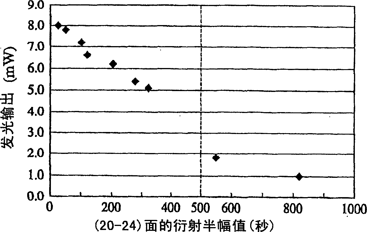
[0037] Even GaN substrates with a small X-ray diffraction half-amplitude on {0002} symmetrical diffraction planes have low luminous luminance of light-emitting diodes (LEDs) using them. substrate formation figure 2 LEDs shown.

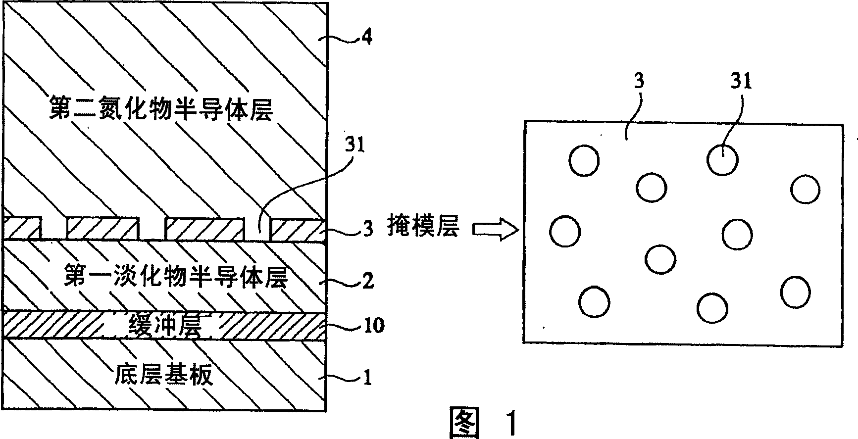
[0038] The manufacturing method of the GaN self-supporting substrate of each sample is as follows. After forming a GaN buffer layer and a GaN layer on a 2-inch-diameter sapphire substrate, the sapphire substrate and GaN buffer layer were removed. Both surfaces of the obtained GaN substrate were polished to produce a GaN self-supporting substrate with a thickness of 270 μm. Manufacturing conditions such as heating temperature were changed for each sample to form a GaN buffer layer and a GaN layer.

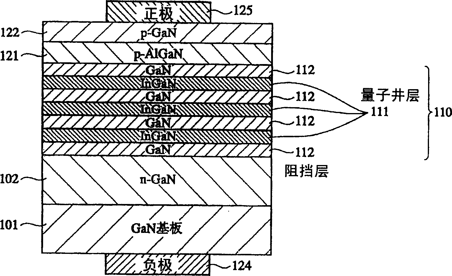
[0039] The structure of the LED formed on each GaN self-supporting substrate is the same as in Example 8 below. Table 1 shows the relationship between the X-ray diffraction half-width of the {0002} plane of the GaN self-supporting substrates of Samples 1...

Embodiment 1

[0042] In the tubular reaction vessel made of quartz provided with a halogen gas supply pipe and a N source supply pipe, a quartz boat containing Ga metal is provided at a position close to the halogen gas supply pipe, and at a position away from the quartz boat and close to For the position of the N source supply pipe, the sapphire base substrate 1 with a diameter of 2 inches perpendicular to the reaction pipe is fixedly arranged on the support.

[0043] While heating the quartz boat containing Ga metal to 900°C, heat the sapphire base substrate 1 to 510°C. In this state, the carrier gas hydrogen and HCl gas are introduced into the tubular reaction vessel from the halogen gas tube, and the tube is supplied from the N source. Supply nitrogen and ammonia as carrier gases. HCl gas reacts with Ga to form GaCl. According to GaCl and NH 3 reaction, a buffer layer made of GaN was grown with a film thickness of 30 nm on the sapphire underlying substrate 1 .

[0044] The temperatur...


PUM

PropertyMeasurementUnit
Thicknessaaaaaaaaaa
Thicknessaaaaaaaaaa
Thicknessaaaaaaaaaa

Abstract

A self-supported nitride semiconductor substrate of 10 mm or more in diameter having an X-ray diffraction half width of 500 seconds or less in at least one of a {20-24} diffraction plane and a {11-24} diffraction plane.

Description

technical field [0001] The present invention relates to a nitride semiconductor self-supporting substrate used for a light-emitting device or the like that obtains high luminous output at a low driving voltage, a method for manufacturing the same, and a nitride semiconductor light-emitting device using the nitride semiconductor self-supporting substrate. Background technique [0002] It is generally difficult to grow nitride semiconductors from molten liquid in bulk. Therefore, after growing nitride semiconductor layers on different types of underlying substrates such as sapphire substrates or gallium arsenide, the underlying substrates are removed and only the nitride semiconductor layers are left to obtain self-supporting. nitride semiconductor substrate. [0003] Nitride semiconductor layers are usually grown on different types of underlying substrates such as sapphire whose crystal lattices do not match well. The nitride semiconductor layer does not grow continuously epi...

Claims


Application Information

Patent Timeline
IPC IPC(8): C30B29/38C30B25/02C30B25/18C30B29/40H01L21/00H01L21/02H01L21/20H01L21/205H01L21/208H01L21/28H01L29/12H01L31/0256H01L33/32
CPCH01L33/16H01L21/0254H01L21/02458H01L21/0242C30B29/40C30B29/403H01L21/02642H01L21/0237C30B25/183H01L33/007H01L21/02502C30B25/02
Inventor 铃木贵征
Owner SUMITOMO CHEM CO LTD
Why Eureka
Try Eureka