Ultraviolet detector with gallium nitride Schottky structure and production thereof

A UV detector, GaN-based technology, used in semiconductor devices, final product manufacturing, sustainable manufacturing/processing, etc. Quantum efficiency, the effect of increasing quantum efficiency, reducing the effect of surface states

Inactive Publication Date: 2005-10-12
INST OF SEMICONDUCTORS - CHINESE ACAD OF SCI
View PDF0 Cites 14 Cited by
  • Summary
  • Abstract
  • Description
  • Claims
  • Application Information

AI Technical Summary

Problems solved by technology

However, due to the existence of surface states (generally speaking, the surface state density is much greater than the interface state density), the photogenerated carriers are easy to recombine on the surface of the Schottky junction, thereby reducing the quantum efficiency of the device and hindering the practical application and application of the device. Further development

Method used


Image

  • Ultraviolet detector with gallium nitride Schottky structure and production thereof
  • Ultraviolet detector with gallium nitride Schottky structure and production thereof
  • Ultraviolet detector with gallium nitride Schottky structure and production thereof

Examples


Embodiment Construction

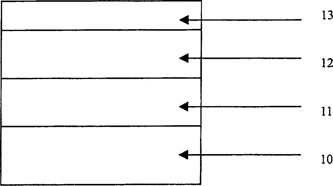
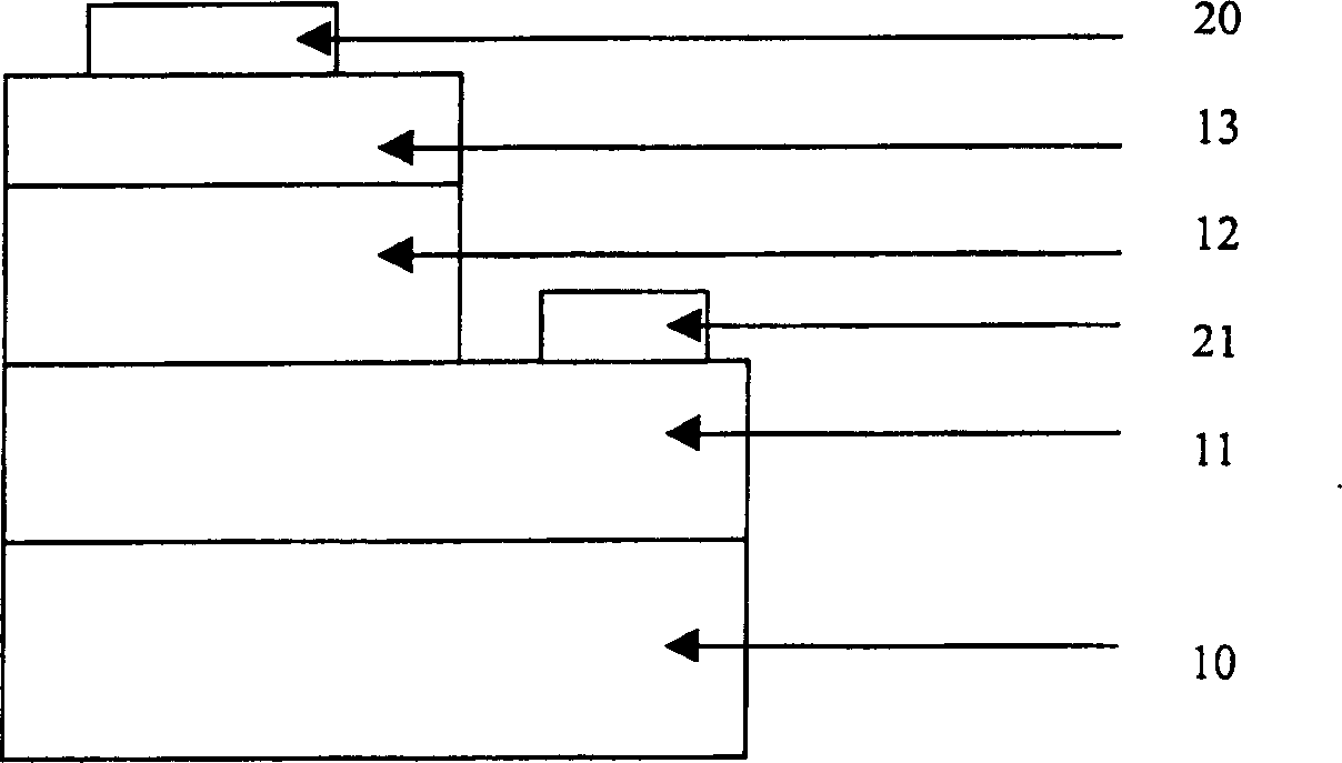
[0037] see figure 1 and figure 2 As shown, a gallium nitride-based Schottky structure ultraviolet detector of the present invention includes:

[0038] A substrate 10, the substrate 10 is made of silicon, sapphire, gallium nitride, gallium arsenide or silicon carbide;

[0039] An ohmic contact layer 11, the ohmic contact layer 11 is made on the substrate 10, the ohmic contact layer 11 is an N-type gallium nitride material with high electron concentration;

[0040] An active layer 12, the active layer 12 is made on the ohmic contact layer 11, the area of ​​the active layer 12 is smaller than the ohmic contact layer 11, and the active layer 12 is an N-type gallium nitride material with low electron concentration;

[0041] A cover layer 13, the cover layer 13 is made on the active layer 12, the cover layer 13 is an N-type aluminum gallium nitride material with low electron concentration, and its aluminum composition is higher than that of the active layer 12;

[0042] An ohmic...


PUM


Abstract

The invention consists of a substrate, an ohmic contact layer, an active layer, a cover layer, an ohmic electrode and two Schottky electrodes. The ohmic contact layer is made on the substrate. The active layer is made on ohmic layer, and has less area than ohmic contact layer. The cover layer is made on active layer. The ohmic electrode is made on the ohmic contact layer. The two Schottky electrodes are made on the cover layer.

Description

technical field [0001] The invention belongs to the field of semiconductor devices, in particular to a novel gallium nitride (GaN)-based Schottky ultraviolet detector structure and a manufacturing method. Background technique [0002] As a third-generation semiconductor, gallium nitride (GaN) and its series of materials (including aluminum nitride, aluminum gallium nitride, indium gallium nitride, and indium nitride) are characterized by their large band gap and wide spectral range (covering from ultraviolet to Infrared full band), high temperature resistance and corrosion resistance, it has great application value in the field of optoelectronics and microelectronics. GaN ultraviolet detector is a very important GaN-based optoelectronic device, which has important application value in civil and military fields such as missile warning, rocket plume detection, ultraviolet communication, biochemical weapon detection, aircraft guidance, spacecraft, and fire monitoring. Compared...

Claims


Application Information

Patent Timeline
Patent Type & Authority Applications(China)
IPC IPC(8): H01L31/108H01L31/18
CPCY02P70/50
Inventor 赵德刚杨辉
Owner INST OF SEMICONDUCTORS - CHINESE ACAD OF SCI
Why Eureka
Try Eureka