Etching technique for preparing ultrathin flexible silicon sustrate through two step method in wet-process etching

A wet etching, silicon substrate technology, used in semiconductor/solid-state device manufacturing, electrical components, circuits, etc., can solve problems such as uneven corrosion

Inactive Publication Date: 2005-11-16
INST OF SEMICONDUCTORS - CHINESE ACAD OF SCI
View PDF0 Cites 10 Cited by
  • Summary
  • Abstract
  • Description
  • Claims
  • Application Information

AI Technical Summary

Problems solved by technology

[0009] However, the current silicon (Si) etching process is not suitable for etching the surface silicon (Si) of flexible silicon substrates, and it is easy to have uneven etching, that is, some areas have been etched to the oxide insulating layer, and some areas are still corroded. There are tens of nanometers of surface silicon (Si)

Method used


Image

  • Etching technique for preparing ultrathin flexible silicon sustrate through two step method in wet-process etching
  • Etching technique for preparing ultrathin flexible silicon sustrate through two step method in wet-process etching
  • Etching technique for preparing ultrathin flexible silicon sustrate through two step method in wet-process etching

Examples


Embodiment

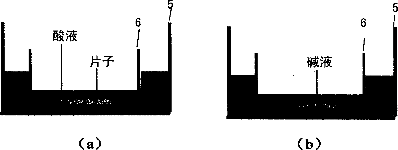
[0040] Imported flexible silicon substrate (SOI) film is prepared by oxygen ion implantation isolation technology, p-type, (100) crystal plane.

[0041] Degreasing treatment: Boil in trichlorethylene-acetone-absolute ethanol for 10-20 minutes in sequence, and wash with deionized water.

[0042] Hydrofluoric acid rinse: Soak in HF solution diluted with water for 10 seconds.

[0043] Acid corrosion: first in HNO 3 Boil in a medium water bath for 2 minutes, wash with deionized water; soak in HF solution for 10 seconds, wash with deionized water; repeat the above operation 3 times.

[0044] After cleaning with deionized water, alkaline etching is performed.

[0045] Alkaline corrosion: ratio, KOH / H 2 O=10g / 100ml (an appropriate amount of ethylene-propanol or n-butanol can be added), corrode at 35°C for 1.5min.

[0046] Under the interference effect of light, the corroded and thinned surface silicon presents a purple-red color with uniform luster (see figure 2 ), with a thick...


PUM


Abstract

The disclosed technique is applicable to thinning down silicon flexible substrate of having oxidation buried layer. Substrate material capable of coordinating mismatched strain is provided for epitaxial growth with large mismatch. The etching technique includes following steps: (1) carrying out degreasing treatment for chip with silicon flexible substrate, cleaning by deionized water, rinsing in diluent hydrofluoric acid, and carrying out ultrathin etching process; (2) first, carrying out acid etching; (3) then, carrying out alkali etching. The invention reaches purpose of uniform etching by using steps of first acid etching and then alkali etching.

Description

technical field [0001] The invention relates to semiconductor technology, which is an etching process for preparing ultra-thin silicon by a two-step wet etching method, which can be used to thin silicon flexible substrates (SOI) with buried oxide layers, and provides a large mismatch epitaxial growth A substrate material that can coordinate mismatch strain. Background technique [0002] New compound semiconductor materials, such as silicon carbide (SiC), gallium nitride (GaN) and zinc oxide (ZnO), have shown very broad application prospects in high temperature, high frequency, high power devices, and optoelectronic devices. However, it is still very difficult to prepare their single crystal materials, and there is a lack of suitable substrate materials for epitaxial growth. [0003] Commonly used substrates are silicon and sapphire. The epitaxial growth of silicon carbide (SiC) (gallium nitride (GaN), zinc oxide (ZnO), etc.) on sapphire (Si) is a large mismatch epitaxial g...

Claims


Application Information

Patent Timeline
Patent Type & Authority Applications(China)
IPC IPC(8): H01L21/306
Inventor 王晓峰曾一平孙国胜黄风义王雷赵万顺
Owner INST OF SEMICONDUCTORS - CHINESE ACAD OF SCI
Why Eureka
Try Eureka