Process for manufacturing photosensitive flat-panel with Se allotropic P.N or N.P structure

A manufacturing process and technology for large flat plates, applied in the field of manufacturing process of large photosensitive flat plates, can solve the problems of the popularization, development and improvement of DR technology, difficulty in obtaining film layers, and runaway temperature of conductive flat plates, etc.

Inactive Publication Date: 2006-02-15
李金根 +2
View PDF0 Cites 0 Cited by
  • Summary
  • Abstract
  • Description
  • Claims
  • Application Information

AI Technical Summary

Problems solved by technology

However, the (a-se) film is very difficult to manufacture, the success rate is low, its repeatability and stability are poor, the charging performance is also unstable, and the potential is not ideal
In addition, because there is no convection in a vacuum environment, there is a gap between the temperature control substrate and the conductive plate, and the radiation conduction effect is poor, so the conduction is blocked and the temperature of the conductive plate is out of control. This is the key reason why it is difficult to obtain an ideal (a-se) film layer
Therefore, the current price of a TFT flat panel detector is about 80,000 to 100,000 dollars. As a consumable, such a price is unacceptable, which greatly limits the popularization, development and improvement of DR technology.

Method used


Image

  • Process for manufacturing photosensitive flat-panel with Se allotropic P.N or N.P structure
  • Process for manufacturing photosensitive flat-panel with Se allotropic P.N or N.P structure
  • Process for manufacturing photosensitive flat-panel with Se allotropic P.N or N.P structure

Examples


Embodiment Construction

[0019] The requirements of this process for vacuum coating equipment:

[0020] 1. The vacuum degree is at 10 -3 ~10 -5 Pa.

[0021] 2. Evaporation boat material and heating method: ①. It can be heated by an aluminum-magnesium alloy boat electric furnace ②. Use a stainless steel boat and short-circuit heating.

[0022] 3. The evaporation boat must have a baffle.

[0023] 4. Temperature control substrate material: silver, red copper, aluminum plate and the same material type pipe plate welding.

[0024] 5. Temperature control method: Two temperature-controlled water baths control two kinds of temperature circulating water to enter the temperature-controlled substrate

[0025] 6. The evaporation method of the evaporation boat: ①. Dynamic cycle ②. Orientation

[0026] Process steps:

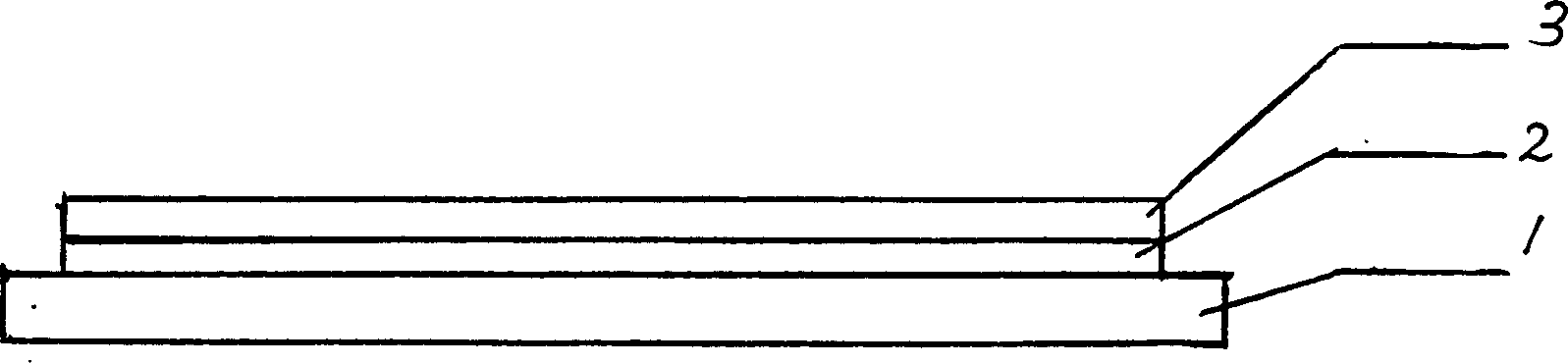
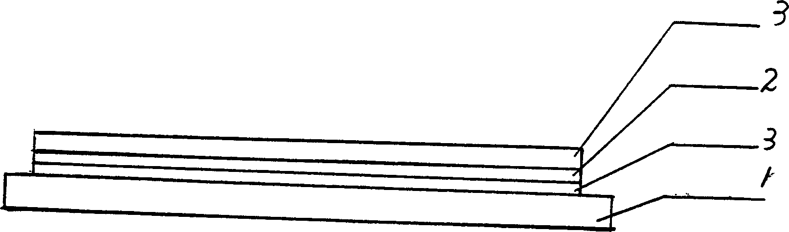
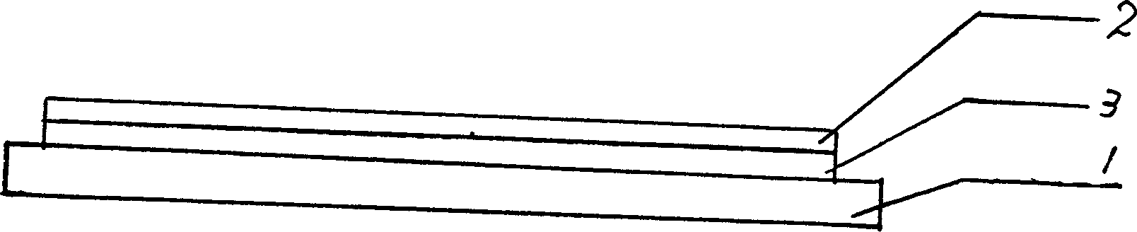
[0027] (a): First clean and dry the conductive plate (conductive plate can be metal plate, glass conductive plate, TFT plate, CMOS plate).

[0028] (b): Put in a vacuum chamber, add heat-condu...


PUM


Abstract

This invention discloses manufacture technique with allotropic P.N or N.P structure for direct imaging sensitization massive plate, which processes the mixing membrane layer of amorphous selenium and crystal selenium, and crystal selenium membrane layer on conducting plate. The invention is new to overcome drawbacks in existing technique, has high stable potential, well imaging quality and repeatability, and benefits to the digitization development of future medical image.

Description

technical field [0001] The invention discloses a manufacturing process of a photosensitive large flat plate in a new medical image digitization technology. Background technique [0002] Currently in the field of medical imaging digital technology, the best is the direct imaging (DR) technology. The most important component in DR technology is a large-scale thin film transistor matrix (TFT) or chip (CMOS) flat panel detector. Its key technology is the manufacture of high-quality amorphous selenium (a-se) film in photosensitive large flat panel. However, the manufacture of (a-se) membrane is very difficult, the success rate is low, its repeatability and stability are poor, the charging performance is also unstable, and the potential is not ideal. In addition, because there is no convection in a vacuum environment, there is a gap between the temperature control substrate and the conductive plate, and the radiation conduction effect is poor, so the conduction is blocked and th...

Claims


Application Information

Patent Timeline
Patent Type & Authority Applications(China)
IPC IPC(8): H01L21/08C23C14/14C23C14/24
Inventor 李金根许梅华李阳
Owner 李金根
Why Eureka
Try Eureka