Focus ring, plasma etching apparatus and plasma etching method

A plasma and etching device technology, applied in the field of focus rings, can solve unresolved problems, achieve the effects of suppressing the reduction of etching rate, high in-plane uniformity, and improved uniformity

Inactive Publication Date: 2006-05-24
TOKYO ELECTRON LTD
View PDF1 Cites 8 Cited by
  • Summary
  • Abstract
  • Description
  • Claims
  • Application Information

AI Technical Summary

Problems solved by technology

This patent document 1 describes that HBr (hydrogen bromide) gas is used as the main component, and SF is added thereto. 6 (sulfur hexafluoride) gas, SiF 4 (Silicon tetrafluoride) gas, and then add He (helium) gas

Method used


Image

  • Focus ring, plasma etching apparatus and plasma etching method
  • Focus ring, plasma etching apparatus and plasma etching method
  • Focus ring, plasma etching apparatus and plasma etching method

Examples


Embodiment

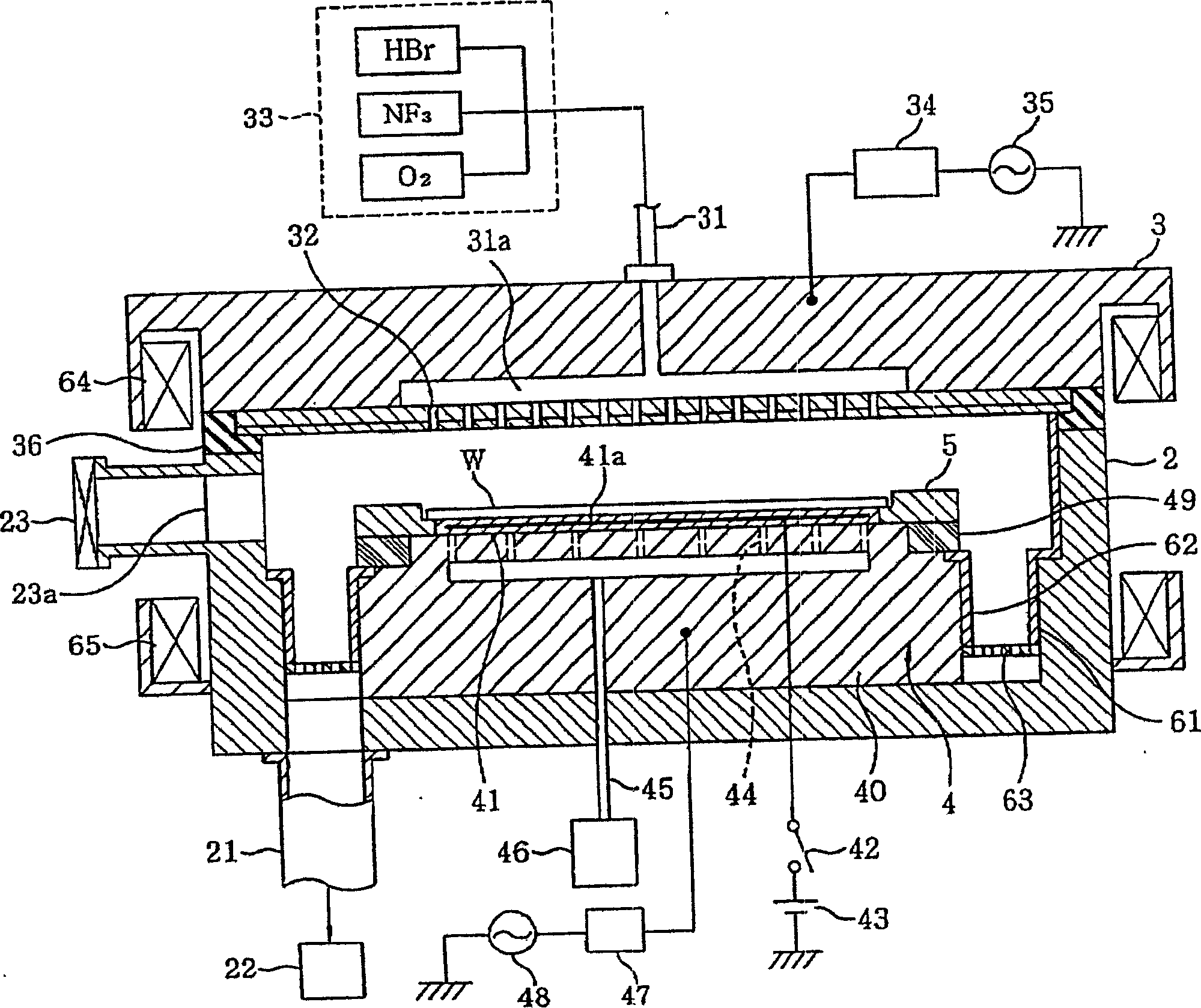
[0049] Next, in order to confirm the effect of this invention, the Example performed is demonstrated. For the focus ring 5 described in the above-mentioned embodiment, the whole surface is processed into a mirror surface, and the average surface roughness Ra is taken as 0.05, and it is installed on figure 1 In the plasma etching device, 1800 pieces with Figure 3A The wafer W on the surface portion shown was grooved individually, and the total etching treatment time was 30 hours. The focus ring 5 was taken out, and the surface was examined. As a result,

[0050] From the inner edge of the focus ring 5 to the area S0 radially outside 5 mm, the average surface roughness Ra is 0.8,

[0051] From the above-mentioned area S0 of the focus ring 5 to the area S1 of 32 mm outside, the average surface roughness Ra is 0.15,

[0052] From the above-mentioned area S1 of the focus ring 5 to an area S2 of 64 mm outside, the average surface roughness Ra was 0.36.

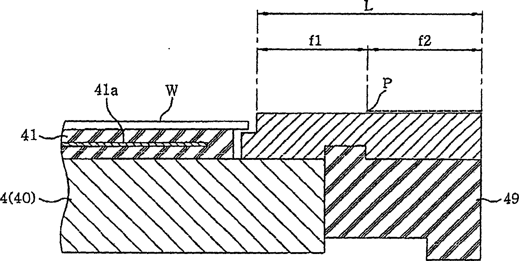
[0053] Figure 5A ~C i...


PUM


Abstract

PROBLEM TO BE SOLVED: To suppress the adhesion of a reaction product at a semiconductor wafer periphery for forming trenches by etching e.g., a silicon layer with plasma to suppress the reduction of an etching rate.

SOLUTION: An inner region on the surface of a focus ring is finish-worked at mean surface roughness Ra in e.g., 0.1 or less as fine as suppressing the adhesion of a reaction product in an etching process, and an outer region is finish-worked at mean surface roughness Ra e.g., 3.2 or less. The boundary between the inner and outer regions is taken as a portion where the level of consumption changes when the focus ring is incorporated in a plasma etcher to etch a substrate with plasma.

COPYRIGHT: (C)2006,JPO&NCIPI

Description

technical field [0001] The present invention relates to a focus ring, a plasma etching apparatus, and a plasma etching method used in a plasma etching apparatus for etching a substrate such as a semiconductor wafer with plasma, for example, forming a groove on the surface of the substrate. Background technique [0002] It is commercially important to incorporate DRAM into logic devices of digital home appliances such as digital TV, DVD recorder, and digital camera, and has become a major form in the semiconductor industry. In the case of logic devices, 0.18μm technology has been used to integrate devices with a scale of 10 million gates on one LSI, and to mount various LSIs including the CPU on a single silicon wafer. System on chip (SOC) . The mixed load technology required to realize SOC is a technology that maximizes the performance of each LST and realizes it with the minimum number of process steps. [0003] The memory cells of the DRAM are arranged at intersections o...

Claims


Application Information

Patent Timeline
IPC IPC(8): H01L21/3065C23F4/00
CPCH01J37/32642H01L21/67069
Inventor 佐藤大树小林秀行堀口将人
Owner TOKYO ELECTRON LTD
Why Eureka
Try Eureka