Production of inverted gallium nitride base light emitting diode chip

A light-emitting diode, gallium nitride-based technology, applied in the direction of electrical components, circuits, semiconductor devices, etc., can solve the problems of small heat dissipation area, affecting the working performance and life of the die

Inactive Publication Date: 2006-05-31
INST OF SEMICONDUCTORS - CHINESE ACAD OF SCI
View PDF0 Cites 12 Cited by
  • Summary
  • Abstract
  • Description
  • Claims
  • Application Information

AI Technical Summary

Problems solved by technology

This preparation method needs to etch the N-type mesa, and the heat dissipat

Method used


Image

  • Production of inverted gallium nitride base light emitting diode chip
  • Production of inverted gallium nitride base light emitting diode chip
  • Production of inverted gallium nitride base light emitting diode chip

Examples


Embodiment Construction

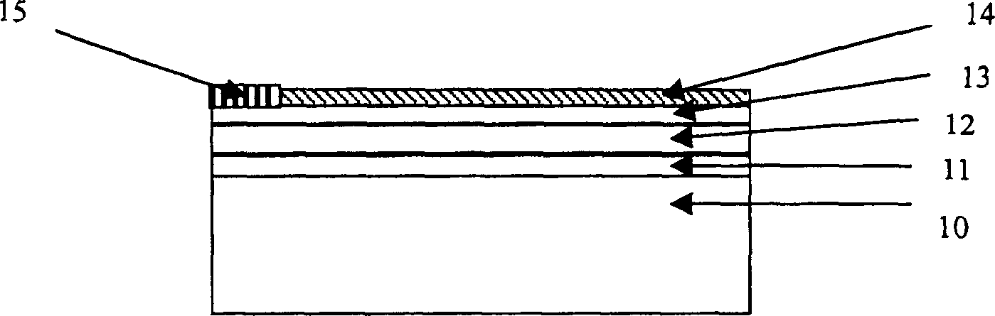
[0023] See first figure 1 As shown, this is a cross-sectional view of a gallium nitride-based light-emitting diode die structure. The manufacturing process is to epitaxially grow a GaN N-type contact layer 11 on a sapphire substrate 10 using MOCVD method, a light-emitting active region 12 and a P-type GaN contact layer 13; the shape of the tube core is designed to be square, with a size of 1mm×1mm, and then a 0.3 micron thick silicon dioxide insulating isolation layer 15 is deposited on the P-type GaN layer 13 by PECVD method according to the designed tube core pattern and size According to the designed chip pattern, a window is etched on the silicon dioxide or silicon nitride insulating layer, and a 0.2 micron thick metal silver (Ag) is prepared by evaporation on the exposed window of the P-type GaN layer, and at 300 Celsius alloy for 5 minutes to form a P-type ohmic contact electrode 14 with high reflectivity. The sapphire substrate is thinned to 100 μm by grinding from the ...


PUM

PropertyMeasurementUnit
Thicknessaaaaaaaaaa
Thicknessaaaaaaaaaa

Abstract

A process for preparing the reverse GaN-based LED chip includes such steps as epitaxial growth of N-type GaN contact layer, active luminescent region and P-type GaN layer on substrate, depositing insulating SiO2 or SiN layer on said P-type layer, thinning the substrate from its back, depositing insulating and isolating SiO2 or SiN layer on carrier, preparing P-type solder bosses on P-type electrode and N-type solder boss on N-type electrode, reversely soldering each chip onto carrier, and cutting for separating the LED chip units from each other.

Description

technical field [0001] The invention belongs to the technical field of semiconductors, in particular to a method for manufacturing a flip-chip gallium nitride-based light-emitting diode chip. Background technique [0002] III-V GaN-based compound semiconductors and their quantum well structure light-emitting diodes (LEDs) have the advantages of high reliability, high efficiency, long life, full solidification, and low power consumption. The field of light display and indication has a huge application market, especially the combination of gallium nitride-based purple or blue light-emitting diodes and phosphors can be made into white light diodes, which has a potential application market in the lighting field and is expected to replace the current incandescent and Fluorescent lamps have become green lighting sources in the 21st century. In order to meet the lighting requirements in the future, GaN light-emitting diode dies can be fabricated using flip-chip welding technology,...

Claims


Application Information

Patent Timeline
IPC IPC(8): H01L33/00
Inventor 李丙乾张书明杨辉
Owner INST OF SEMICONDUCTORS - CHINESE ACAD OF SCI
Why Eureka
Try Eureka