Crystal tube structure with high electronic shifting ratio of gallium nitrate base of double heterogenous structure and mfg. method thereof

A high electron mobility, double heterostructure technology, applied in semiconductor/solid state device manufacturing, circuits, electrical components, etc., can solve problems such as channel current reduction, channel electron concentration reduction, current collapse, etc.

Inactive Publication Date: 2006-06-14
INST OF SEMICONDUCTORS - CHINESE ACAD OF SCI
View PDF0 Cites 9 Cited by
  • Summary
  • Abstract
  • Description
  • Claims
  • Application Information

AI Technical Summary

Problems solved by technology

At present, there are many controversies about the cause of the current collapse effect of AlGaN / GaN HEMT devices. One of the more convincing ones is the virtual gate model, that is, under the radio frequency signal, the channel electrons are captured by the trap center on the surface of the AlGaN barrier layer. The concentration of electrons in the channel is reduced, and the surface state captures electrons to form a virtual gate, which modulates the channel current, causing the channel current to decrease, forming a current collapse; the second is the high-resistance GaN buffer layer model, when the field is high, The channel electrons are captured by the trap center of the high-resistance (semi-insulating) GaN buffer layer, resulting in a decrease in the channel electron concentration and a decrease in the channel current, forming a current collapse

Method used


Image

  • Crystal tube structure with high electronic shifting ratio of gallium nitrate base of double heterogenous structure and mfg. method thereof
  • Crystal tube structure with high electronic shifting ratio of gallium nitrate base of double heterogenous structure and mfg. method thereof
  • Crystal tube structure with high electronic shifting ratio of gallium nitrate base of double heterogenous structure and mfg. method thereof

Examples


Embodiment

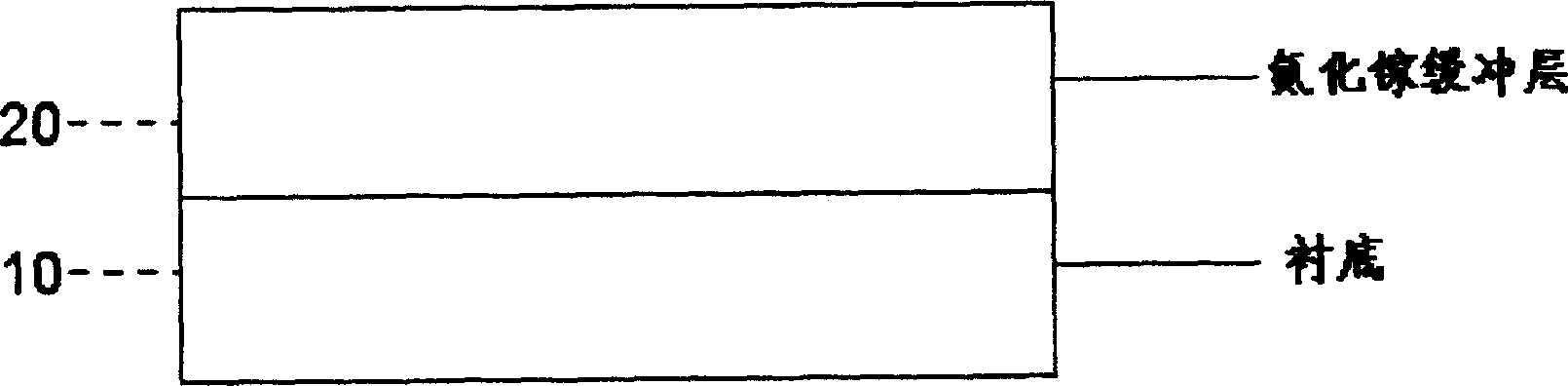
[0062] Examples (see Figure 3-Figure 7 ):

[0063] (1) First, a thicker high-resistance (semi-insulating) GaN buffer layer 20 is grown on the substrate sapphire 10 (0001) crystal surface by molecular beam epitaxy technology, the growth temperature is about 1000 ° C, and the growth thickness is about 1.5 -3.5μm, ( image 3 ) The high-resistance (semi-insulating) gallium nitride buffer layer 20 can be generated by ion implantation, doping, compensation, etc., the main purpose is to reduce the leakage of the buffer layer of the current during device operation, and prevent the performance deterioration caused by the increase in device operating temperature , improve the stability of the device.

[0064] (2), secondly on the high resistance (semi-insulating) gallium nitride buffer layer 20, grow a thin layer of aluminum gallium nitride (Al x Ga 1-x N, 0 Figure 4 ) According to needs, the Al composition x of the AlGaN insertion layer 30 can be between 0


PUM

PropertyMeasurementUnit
thicknessaaaaaaaaaa
thicknessaaaaaaaaaa
thicknessaaaaaaaaaa

Abstract

The invention is a double-heterostructured GaN-base high-electron migration rate transistor structure, characterized in comprising: a sapphire, silicon carbide or silicon substrate; a high resistance GaN buffer layer made on the substrate; a thin unpurposed doped GaN insert layer made on the buffer layer; a high-migration rate GaN channel layer made on the thin unpurposed doped GaN insert layer; a thin AlN insert layer made on the channel layer; a n-type doped or unpurposed doped Al-Ga-N barrier layer made on the thin AlN insert layer.

Description

technical field [0001] The invention belongs to the technical field of semiconductors, in particular to the structure and manufacturing method of a novel double-heterostructure aluminum gallium nitride / gallium nitride high electron mobility transistor (AlGaN / GaN HEMT). Background technique [0002] The AlGaN / GaN high electron mobility transistor structure formed by III-V gallium nitride (GaN) and its compound semiconductor materials has very important application prospects in the fields of high-temperature, high-frequency, high-power, radiation-resistant microwave devices and circuits. Mainly because the semiconductor material that makes up the AlGaN / GaN heterostructure has a large band gap, high breakdown electric field, good chemical stability and strong radiation resistance, and also because the GaN material has a high electron saturation drift velocity and peak drift velocity, more importantly because a two-dimensional electron gas with high electron concentration and hi...

Claims


Application Information

Patent Timeline
Patent Type & Authority Applications(China)
IPC IPC(8): H01L29/737H01L21/331
Inventor 王晓亮王翠梅胡国新王军喜李建平曾一平李晋闽
Owner INST OF SEMICONDUCTORS - CHINESE ACAD OF SCI
Why Eureka
Try Eureka