

Structure for improving Schottky performance of grid electrode of gallium nitride based transistor in high electron mobility
A high electron mobility, gallium nitride-based technology, applied in the semiconductor field, can solve the problems of reducing the quality of AlGaN/GaNHEMT device gate Schottky junction, affecting the performance of AlGaN/GaNHEMT devices, etc.
- Summary
- Abstract
- Description
- Claims
- Application Information
AI Technical Summary
Problems solved by technology
Method used
Image

Examples
Embodiment
[0030] Examples (see Figure 2-Figure 7 ):
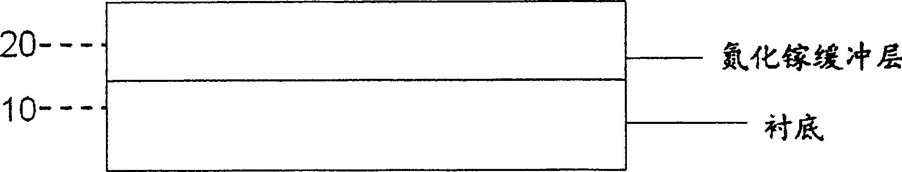
[0031] (1) First, a thicker high-resistance (semi-insulating) gallium nitride buffer layer 20 is grown on the (0001) crystal surface of the substrate sapphire 10 by molecular beam epitaxy technology, the growth temperature is 1050° C., and the growth thickness is 1.5-5 μm. ( figure 2 ) The high-resistance (semi-insulating) gallium nitride buffer layer 20 can be generated by methods such as ion implantation, doping, compensation, etc., and the main purpose is to reduce the leakage of the buffer layer of the current when the device is in operation, thus preventing the device from operating temperature rise. Performance deterioration improves device stability.
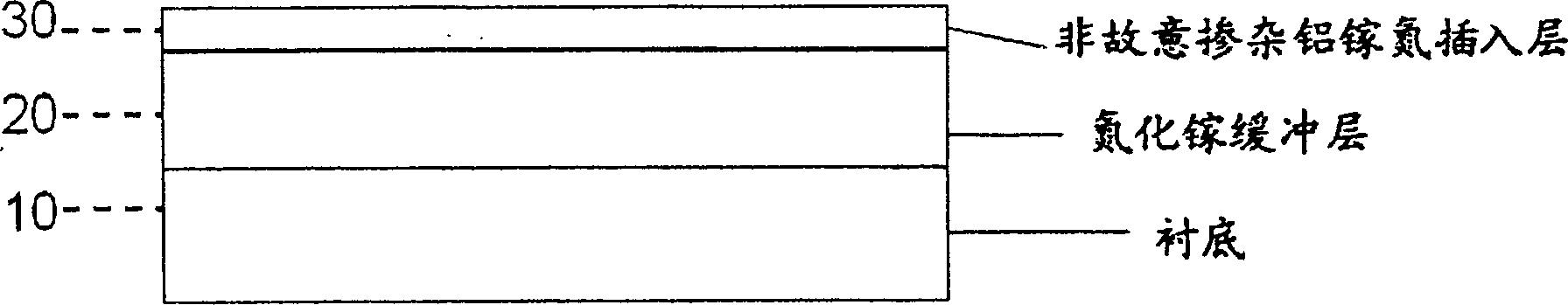
[0032] (2) Second, grow a thin layer of non-intentionally doped AlGaN (Al x Ga 1-x N, 0≤x≤1) the insertion layer 30 has a thickness of 1-10 nm, ( image 3 ) According to needs, the Al composition x of the unintentionally doped AlGaN insertion layer 30 can be changed betwee...
PUM
| Property | Measurement | Unit |
|---|---|---|
| Thickness | aaaaa | aaaaa |
| Thickness | aaaaa | aaaaa |
| Thickness | aaaaa | aaaaa |
Abstract
Description
Claims
Application Information