Process for preparing functional film on fused substrate surface

A substrate surface and thin film technology, which is applied in the field of preparation of functional thin films, can solve the problems of undisclosed key parameters and achieve the effects of overcoming microstructure instability, simple preparation process, and low cost

Inactive Publication Date: 2006-07-26
ZHEJIANG UNIV
View PDF0 Cites 2 Cited by
  • Summary
  • Abstract
  • Description
  • Claims
  • Application Information

AI Technical Summary

Problems solved by technology

However, the details of the specific preparation method, the selection of film materials and key parameters are not disclosed, for example, the minimum deposition rate when growing films of different materials; the heating and holding time of the substrate; the choice of liquid-phase substrate materials; the schematic diagram of the experiment, etc., to implement the method creative labor

Method used


Image

  • Process for preparing functional film on fused substrate surface

Examples


Embodiment 1

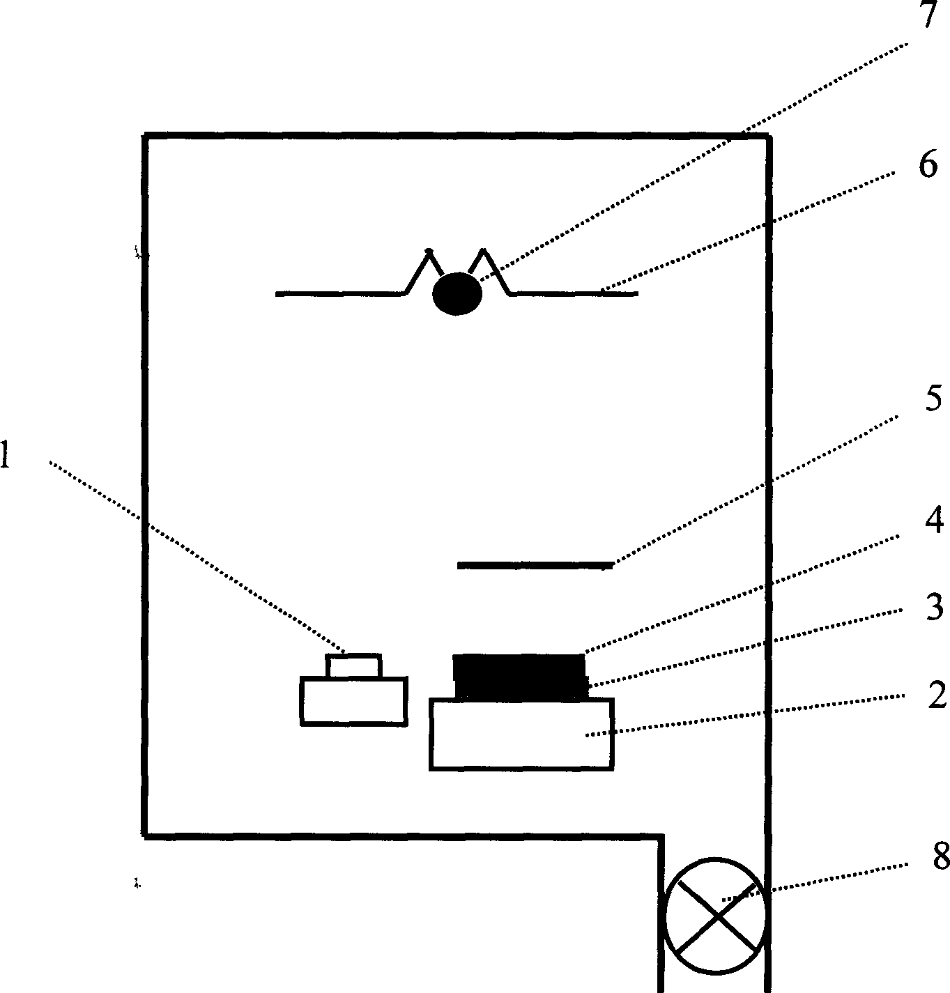
[0034] (a) refer to figure 1 , in the vacuum chamber of the vacuum evaporation device, a small amount of low-melting point and low-melting vapor pressure substrate material 4 is placed on the frosted glass slide 3, and the substrate frame is formed together with the electric furnace 2 for controlling the substrate temperature, and the low-melting point and low-melting The vapor pressure base material can be one of low melting point glass and low melting point polymer material; the evaporation source is composed of the evaporation material 7 and the heating tungsten wire 6, and the material of the evaporation source can be non-magnetic material Au with a purity of 99.9% to 99.99%. , Ag, Al, Cu or one of the magnetic materials Fe, Ni. The base surface of the film on the substrate frame faces the evaporation source, and the distance between the substrate frame and the evaporation source is 8-15 cm, and they are separated by a baffle plate 5 . The crystal oscillator thickness gau...

Embodiment 2

[0041] A gold film is deposited on the surface of an insulating substrate with a low melting point and low melting vapor pressure by radio frequency magnetron sputtering:

[0042] (a) In the vacuum chamber of radio frequency magnetron sputtering, the substrate is made of low melting point and low vapor pressure glass with a melting temperature of 500°C, and the sputtering target material (ie thin film material) has a purity equal to 99.99%, a diameter of 81.5mm, and a thickness of 0.5mm pure gold (Au) sheet material, the distance between the substrate holder and the sputtering target is 8cm, and they are separated by a baffle.

[0043] (b) Evacuate the chamber to 6×10 with mechanical pump and molecular pump -4 Pa vacuum.

[0044] (c) Heating the substrate to 510° C. with an electric furnace to melt the glass substrate into a liquid phase (colloid) substrate whose vapor pressure is lower than that in the vacuum chamber.

[0045] (d) Increase the sputtering power to about 10W,...


PUM

PropertyMeasurementUnit
sizeaaaaaaaaaa
thicknessaaaaaaaaaa
particle sizeaaaaaaaaaa

Abstract

The invention discloses a functional film preparing method of molten substrate surface, which is characterized by the following: adopting the material of solid-phase low-melting point and low vapor pressure at ambient temperature; elevating substrate temperature before depositing film; melting film for liquid phantom background; evaporating film material atom and depositing to liquid level substrate surface with the method of magnetron sputtering or heat evaporation; adopting the method of diffusing, formatting the core, rolling, aggregating to grow functional film of characteristic grain arrangement; reducing substrate temperature to room temperature after finishing aggradation; curing background; keeping microconfiguration of film stable. The method simplifies technique, which reduces the cost.

Description

technical field [0001] The invention belongs to the technical field of preparation of nanoparticles, nanocrystal grains, high-strength adhesion between films and substrates, and functional films with characteristic microstructures, and specifically relates to a new film preparation technology: low melting point and low The vapor pressure material is the substrate; before depositing the film, the temperature of the substrate is raised to melt it into a liquid phase substrate; after the deposition is completed, the temperature of the substrate is freely cooled to room temperature, and the substrate is solidified, so that the microstructure of the film is maintained stably . Background technique [0002] In the past few decades, brilliant achievements have been made in thin film science and technology research, and new functional thin films with various unique functions emerge in an endless stream, such as the mature superconducting thin film in the 1970s, the superlattice thin...

Claims


Application Information

Patent Timeline
Patent Type & Authority Applications(China)
IPC IPC(8): C23C14/22C23C14/24C23C14/35C23C14/54C23C14/56C23C14/58C23C14/02
Inventor 叶高翔
Owner ZHEJIANG UNIV
Why Eureka
Try Eureka