Non-aluminium 1.3 micron indium arsenic/gallium arsenic quantum point laser

A quantum dot and laser technology, applied in the field of aluminum-free 1.3μm indium arsenide/gallium arsenide quantum dot lasers, can solve the problems of deterioration of QDs laser temperature characteristics, lowering of limiting barriers, device application limitations, etc., to achieve low defect concentration and Effect of Surface Recombination Rate, Interdiffusion Inhibition, and Device Quality Improvement

Inactive Publication Date: 2006-08-30
INST OF SEMICONDUCTORS - CHINESE ACAD OF SCI
View PDF0 Cites 7 Cited by
  • Summary
  • Abstract
  • Description
  • Claims
  • Application Information

AI Technical Summary

Problems solved by technology

This reduces the confinement barrier on both sides of the QDs, reduces the energy level difference between the ground state and the excited state of the QDs, and leads to deterioration of the temperature characteristics of the QDs laser.
The application of InAlAs / InGaAs composite stress buffer layer or composite stress capping layer can solve this contradiction to a certain extent, but due to the above-mentioned shortcomings of aluminum-containing materials, the application of devices is limited

Method used


Image

  • Non-aluminium 1.3 micron indium arsenic/gallium arsenic quantum point laser
  • Non-aluminium 1.3 micron indium arsenic/gallium arsenic quantum point laser
  • Non-aluminium 1.3 micron indium arsenic/gallium arsenic quantum point laser

Examples


Embodiment

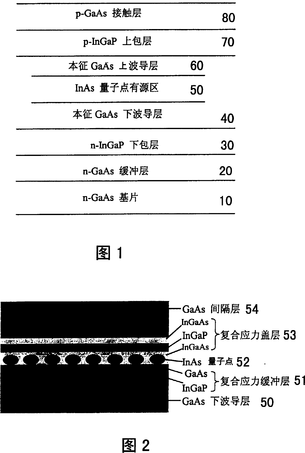
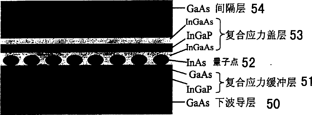
[0052] See Figure 1 and Figure 2:

[0053]1) The washed GaAs substrate 10 is placed in an MOCVD reaction chamber, and a GaAs buffer layer 20 of about 500 nanometers is grown (the reaction chamber temperature is 600 degrees Celsius);

[0054] 2) On the GaAs buffer layer 20, grow n-doped indium gallium phosphide (In 0.49 Ga 0.51 P) The lower cladding layer 30 is grown at a temperature of 530-570 degrees Celsius, and then a 100 nm undoped GaAs lower waveguide layer 40 is grown at the same temperature.

[0055] 3) Epitaxially growing the QDs active region 50 on the lower waveguide layer. The active region 50 is InAS quantum dots 52 of 3-5 periods separated by a 30 nm thick GaAs layer, and the growth temperature is 50

[0056] 0-515 degrees Celsius. In order to extend the emission wavelength of the quantum dots 52 and increase the confinement barrier to increase the characteristic temperature of the device, an InGaP / GaAs composite stress buffer layer 51 and an InGaP / InGaAs comp...


PUM

PropertyMeasurementUnit
Thicknessaaaaaaaaaa
Thicknessaaaaaaaaaa
Thicknessaaaaaaaaaa

Abstract

This invention relates to a 1.3mum InAs / GaAs quantum dot laser without Al including a chip, a buffer layer processed on the chip, a lower cladding made on the buffer layer, a lower waveguide layer set on the lower cladding, a quantum dot active region set on the lower waveguide layer, an upper waveguide layer prepared on the active region of the quantum dot, an upper cladding prepared on the upper waveguide layer under low temperature, a contact layer prepared on the upper cladding. Since high quality of the InGaP can be got under low growing temperature, the blue shift of the quantum dots is controlled effectively in the growing process of the cladding.

Description

technical field [0001] The invention relates to an indium arsenide (InAs) / gallium arsenide (GaAs) quantum dot (QDs) laser grown by metal organic compound vapor phase epitaxy (MOCVD), in particular to an aluminum-free 1.3 μm indium arsenic / gallium arsenic quantum dot laser. Background technique [0002] It is theoretically predicted that lasers with QDs as the active region have superior properties such as high quantum efficiency, low threshold current and high characteristic temperature. Recently, InAs / GaAs QDs grown on GaAs substrates have attracted extensive attention because they can extend the laser emission wavelength to 1.3 μm or 1.5 μm. There have been many studies on InAS QDs 1.3 μm lasers grown by molecular beam epitaxy (MBE) technology and realized room temperature work (see Electron.Lett., Vol.40, No.22, 2004, pp 1412-1413 and IEEE Photonics Technol . Lett., Vol.12, No.6, 2000, pp 591-592). Although compared with MBE technology, MOCVD technology has the advanta...

Claims


Application Information

Patent Timeline
IPC IPC(8): H01S5/343H01S5/00
Inventor 梁松朱洪亮
Owner INST OF SEMICONDUCTORS - CHINESE ACAD OF SCI
Why Eureka
Try Eureka