

Method for preparing glass waveguide by ion mask
A technology of optical waveguide and mask, which is applied in the direction of optical waveguide and light guide, can solve the problems that cannot completely prevent high polarizability ions from entering the glass substrate and affect the performance of optical waveguide devices, and achieve the effect of easy implementation and improved performance
- Summary
- Abstract
- Description
- Claims
- Application Information
AI Technical Summary
Problems solved by technology
Method used
Image

Examples
Embodiment 1
[0030] Example 1: Fabrication of optical waveguides using low-temperature ion exchange technology
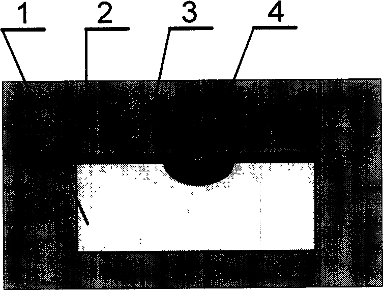
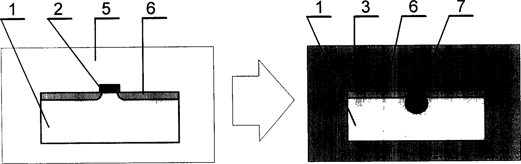
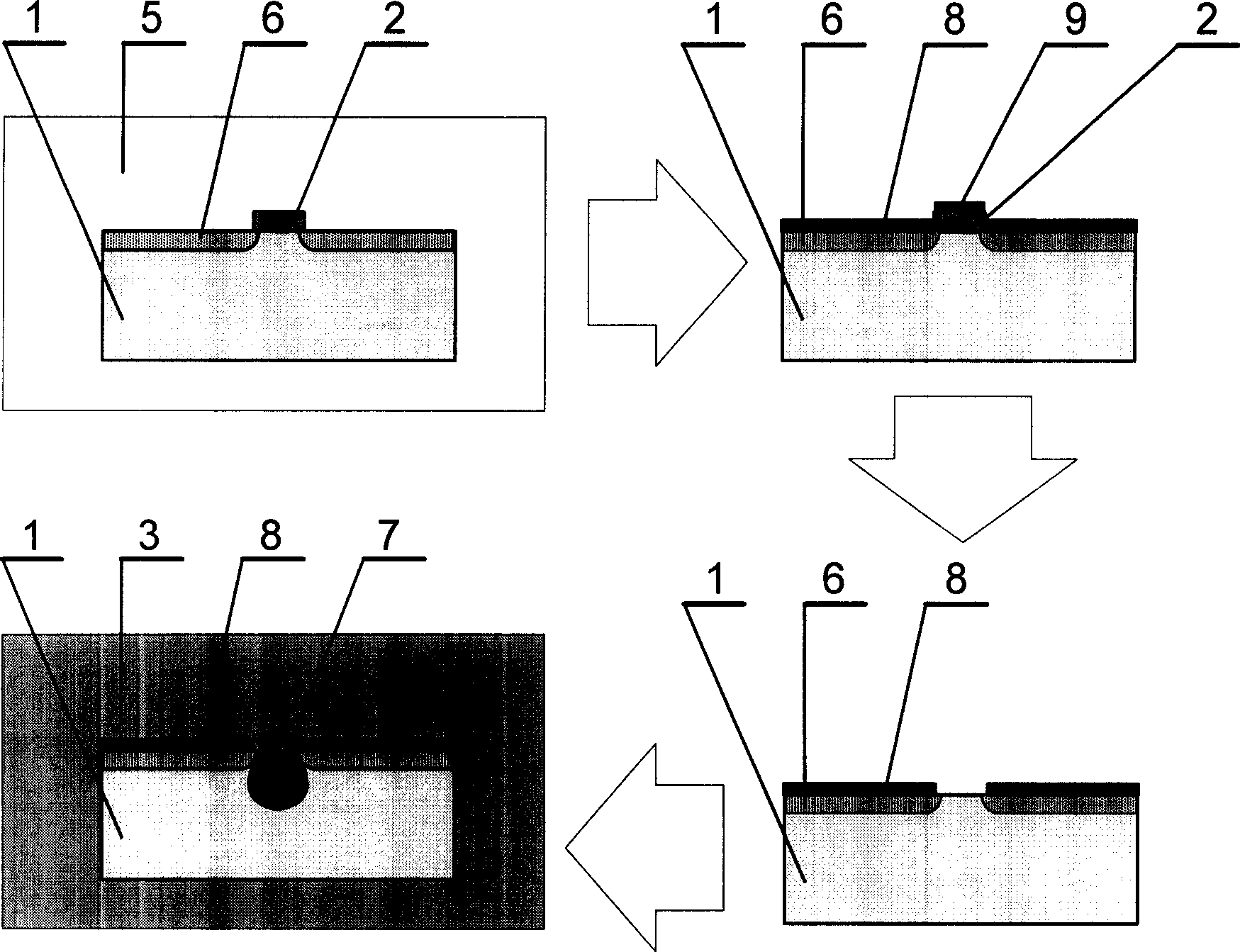
[0031] (1) Make an Al film with a thickness of 150-200nm on the front of the glass substrate by evaporation or sputtering, and then form an ion exchange window on the mask by photolithography and corrosion processes, and then place the glass substrate with the mask Piece into KNO 3 Ion exchange is carried out in the molten salt, the exchange temperature is 320 ° C, the exchange time is 10 hours, the K in the molten salt + K is formed in the glass substrate by thermal diffusion + ion diffusion area.
[0032] (2) After the glass substrate and the Al mask on the surface are cleaned, an Ag thin film with a thickness of 60-120 nm is fabricated on the glass substrate by evaporation or sputtering process.
[0033] (3) Put the glass substrate into dilute hydrochloric acid to etch the Al mask.
[0034] (4) Put the glass substrate with Ag thin film on the surface into AgNO 3 with NaN...
Embodiment 2
[0036] Example 2: Fabrication of an optical waveguide using a medium temperature ion exchange process
[0037] (1) Make an Al film with a thickness of 150-200nm on the front of the glass substrate by evaporation or sputtering, and then form an ion exchange window on the mask by photolithography and corrosion processes, and then place the glass substrate with the mask Piece into KNO 3 Ion exchange is carried out in the molten salt, the exchange temperature is 400 ° C, the exchange time is 5 hours, the K in the molten salt + K is formed in the glass substrate by thermal diffusion + ion diffusion area.
[0038] (2) After the glass substrate and the Al mask on the surface are cleaned, an Ag thin film with a thickness of 60-120 nm is fabricated on the glass substrate by evaporation or sputtering process.
[0039] (3) Put the glass substrate into dilute hydrochloric acid to etch the Al mask.
[0040] (4) Put the glass substrate with Ag thin film on the surface into AgNO 3 with ...
Embodiment 3
[0041] Example 3: Fabrication of an optical waveguide using a medium-temperature ion-exchange process
[0042] (1) Make an Al film with a thickness of 150-200nm on the front of the glass substrate by evaporation or sputtering, and then form an ion exchange window on the mask by photolithography and corrosion processes, and then place the glass substrate with the mask Piece into KNO 3 Ion exchange is carried out in the molten salt, the exchange temperature is 450 ° C, the exchange time is 1 hour, the K in the molten salt + K is formed in the glass substrate by thermal diffusion + ion diffusion area.
[0043] (2) After the glass substrate and the Al mask on the surface are cleaned, an Ag thin film with a thickness of 60-120 nm is fabricated on the glass substrate by evaporation or sputtering process.
[0044] (3) Put the glass substrate into dilute hydrochloric acid to etch the Al mask.
[0045] (4) Put the glass substrate with Ag thin film on the surface into AgNO 3 with N...
PUM
| Property | Measurement | Unit |
|---|---|---|
| Thickness | aaaaa | aaaaa |
Abstract
Description
Claims
Application Information