Semiconductor device and semiconductor device manufacturing method

A manufacturing method and semiconductor technology, applied in semiconductor/solid-state device manufacturing, semiconductor devices, transistors, etc., can solve problems such as increased leakage current, increased power consumption, transistor damage, etc., to improve withstand voltage characteristics, improve rise characteristics, reduce The effect of power consumption

Inactive Publication Date: 2007-01-24
SEIKO EPSON CORP +1
View PDF1 Cites 23 Cited by
  • Summary
  • Abstract
  • Description
  • Claims
  • Application Information

AI Technical Summary

Problems solved by technology

Therefore, there is a problem that the flatness of the base insulating film on which the upper silicon thin film is formed is deteriorated, and there are restrictions on the heat treatment conditions when forming the upper silicon thin film, and the crystallinity of the upper silicon thin film is inferior to that of the lower silicon thin film.
[0007] Furthermore, in conventional semiconductor integrated circuits, when the channel length is shortened with the miniaturization of transistors, the rise characteristics of the drain current in the subthreshold region will deteriorate.
Therefore, there is a problem that while the low-voltage operation performance of the transistor is affected, the leakage current at the time of cut-off is increased, which not only causes an increase in power consumption during operation and standby, but also becomes a main cause of damage to the transistor.

Method used


Image

  • Semiconductor device and semiconductor device manufacturing method
  • Semiconductor device and semiconductor device manufacturing method
  • Semiconductor device and semiconductor device manufacturing method

Examples


Embodiment Construction

[0036] Hereinafter, a semiconductor device and a manufacturing method thereof according to an embodiment of the present invention will be described with reference to the drawings.

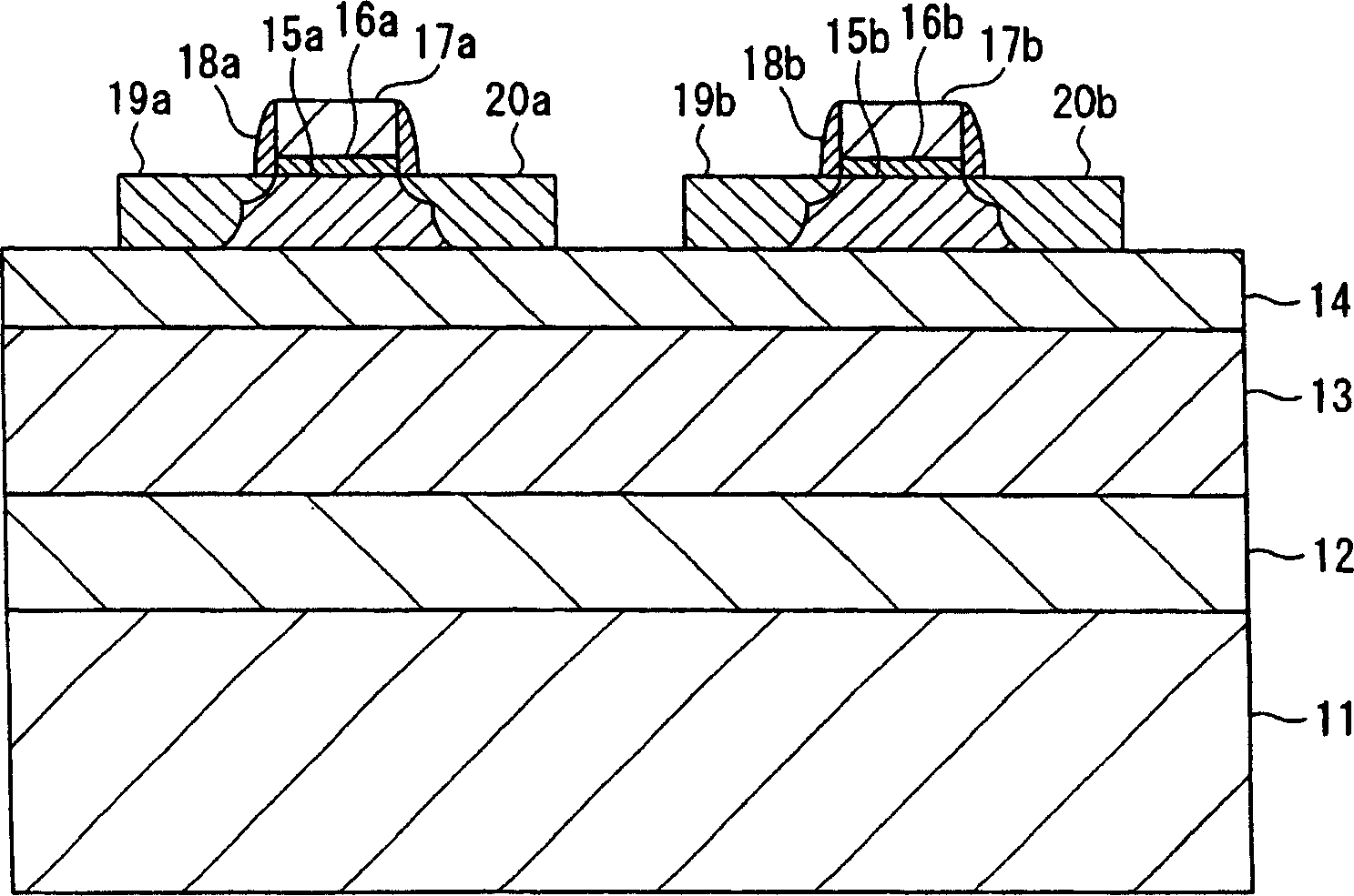
[0037] figure 1 It is a cross-sectional view showing a schematic configuration of the semiconductor device according to the first embodiment of the present invention.

[0038] exist figure 1 In this method, a buried oxide film 12 is formed on a single crystal semiconductor substrate 11, and a first single crystal semiconductor layer 13 constituting a back gate electrode is formed on the buried oxide film 12. Furthermore, a buried oxide film 14 is formed on the first single crystal semiconductor layer 13 . On the buried oxide film 14, second single crystal semiconductor layers 15a, 15b separated by mesas are stacked. In addition, Si can be used as the material of the single crystal semiconductor substrate 11, the first single crystal semiconductor layer 13, and the second single crystal semicondu...


PUM


Abstract

To dispose a back gate electrode forced to have a low resistance under a semiconductor layer to form thereon field effect transistors, while preventing the degradation of the crystal quality of the semiconductor layer to form thereon the field effect transistors. With respect to a semiconductor device, a buried oxide film 12 is formed on a single-crystal semiconductor substrate 11, and a first single-crystal semiconductor layer 13 constituting a back gate electrode is formed on the buried oxide film 12. Further, a buried oxide film 14 is formed on the first semiconductor layer 13, and second single-crystal semiconductor layers 15a, 15b subjected to a mesa-isolation are laminated on the buried oxide film 14. The film thicknesses of the second semiconductor layers 15a, 15b are made larger than that of the first semiconductor layer 13, and SOI transistors are formed respectively on the second semiconductor layers 15a, 15b.

Description

technical field [0001] The invention relates to a semiconductor device and a method for manufacturing the semiconductor device, which are particularly suitable for use in a method for forming a back gate electrode of an SOI (Silicon On Insulator) transistor. Background technique [0002] Field-effect transistors formed on SOI (Silicon On Insulator) substrates have drawn much attention for their usefulness due to their features such as ease of element isolation, no latch up free, and small source / drain junction capacitance. [0003] In addition, for example, in Patent Document 1, a method is proposed in which, in order to form a silicon thin film with good crystallinity and uniformity on a large-area insulating film, an amorphous or The polysilicon layer is irradiated in a pulse shape with an ultraviolet ray beam to form a polysilicon film in which approximately square single crystal grains are arranged in a checkerboard shape on the insulating film, and then the polysilicon ...

Claims


Application Information

Patent Timeline
Patent Type & Authority Applications(China)
IPC IPC(8): H01L29/786H01L27/12H01L21/336H01L21/84
Inventor 加藤树理冈秀明金本启原寿树酒井彻志
Owner SEIKO EPSON CORP
Why Eureka
Try Eureka