
Eureka
For R&D, Eureka makes reading and utilizing patents & technical documents easy.
Eureka AIR
Designed for self-driven R&D workflows. Generate viable solutions, solve complex R&D challenges, empower your innovation with AI.

Eureka Materials
Designed for material experts only. Revolutionize your material R&D, from search, analyze, to developing new materials.

TechResearch
Generate reliable direction feasibility study reports for your R&D in just a few steps.

TechSeek
Discover and master advanced knowledge NOW. Basics, ideas, possibilities, all at once.

TechMind
As an expert in R&D Theories, TechMind can generates customized viable solutions instantly.

TechRisk
Analyze your overall solution with one click, know your potential R&D risks in advance.

TechMonitor
Get weekly tech updates, stay abreast of the latest tech innovations and key insights.
Organic electroluminescence device
An electroluminescent device, an organic technology, applied in the direction of electric solid devices, electrical components, semiconductor devices, etc., can solve the problems of activity damage, reduced visible light transmittance, etc., to reduce exciton quenching centers and increase electron efficiency. Injection area, the effect of improving efficiency
- Summary
- Abstract
- Description
- Claims
- Application Information
AI Technical Summary
Problems solved by technology
Method used
Image

Examples
Embodiment 1
[0022] The prepared structure is ITO / NPB 50nm / Alq 3 50nm / cathode buffer / Al 100nm devices.
[0023]The etched ITO glass is used as the substrate of the OLED, and the cleaning process is as follows: ultrasonically clean once with 60°C deionized water containing surfactant, then ultrasonically rinse twice with 60°C clean deionized water, and rinse with cold deionized water Ultrasonic rinsing twice, drying in a clean bench with infrared light. All films were prepared by thermal evaporation in a vacuum chamber with a background pressure of 1.0×10 -3 Pa, the light emitting area of the device is 3×3mm 2 . 50nm thick N,N'-diphenyl-N,N'-bis(1-naphthyl)-1,1'-biphenyl-4,4'-diamine (NPB) was used as the hole transport layer, which The evaporation rate is 0.1nm / s; the 50nm-thick tris(8-hydroxyquinoline)aluminum is used as the electron transport layer and the light-emitting layer, and the evaporation rate is 0.1nm / s. After the evaporation of the organic layer is completed, the devic...
Embodiment 2
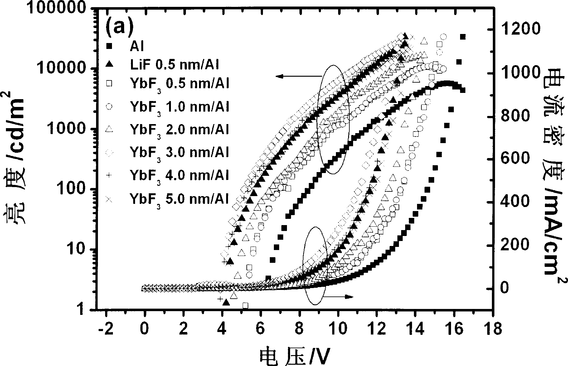
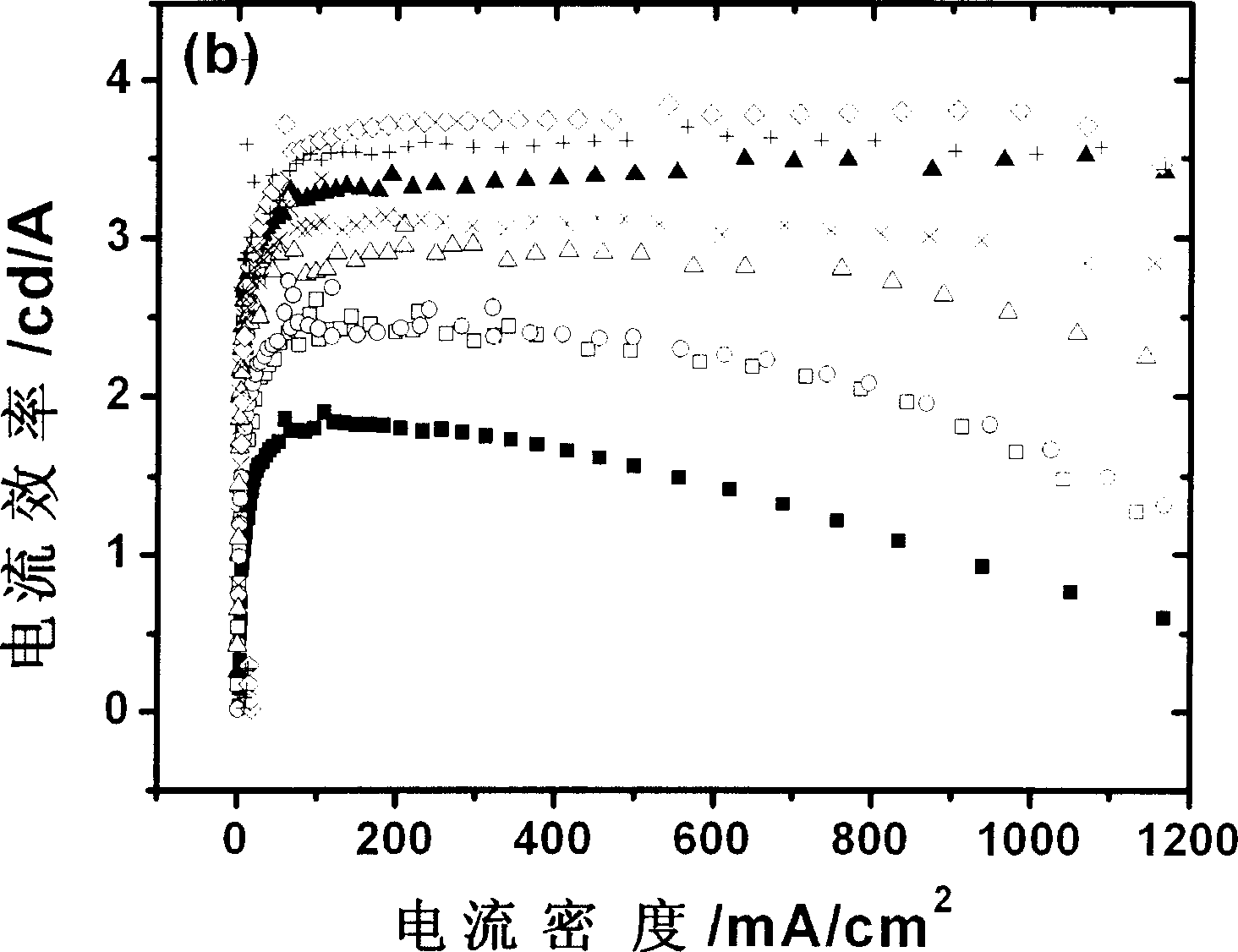
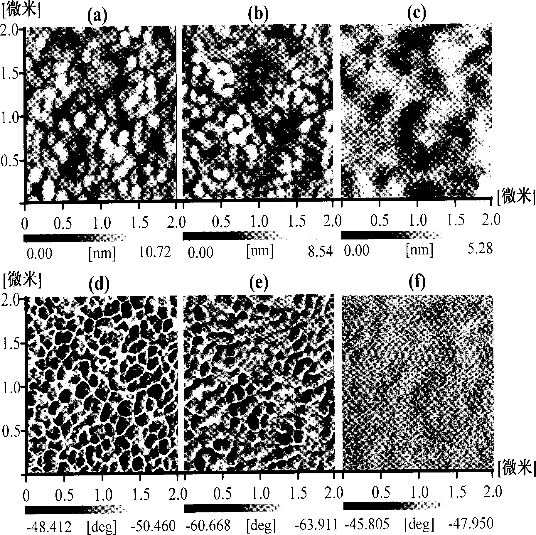
[0032] Devices were prepared according to the method of Example 1, all films were prepared by vacuum evaporation, wherein the cathode buffer layer material was replaced by YbF 3 / Yb, the evaporation rate is 0.03-0.05nm / s, and the thickness range is 0.5nm-30nm. The optimal thickness of the cathode buffer layer material is 3.0nm / 14.5nm, and the brightness of the device reaches 1cd / m2 at 3.6V under the drive of DC voltage 2 , the device current density is 500mA / cm at 10.8V 2 , the brightness is 11560cd / m 2 . The injection mechanism is the cathode buffer layer YbF 3 Chemically react with the hot atoms of Yb activated by vacuum evaporation to generate Yb at the interface, doped into the organic layer to form Alq which is conducive to electron injection 3 negative ions, which lowers the electron injection barrier, while YbF 3 The organic layer is protected from being damaged by Yb thermal atoms.
[0033] Device Cathode Structure
[0034] From the above two examples we...
Embodiment 3
[0036] Devices were prepared according to the method of Example 1, all films were prepared by vacuum evaporation, wherein the cathode buffer layer material was replaced by YbF 2 , the evaporation rate is 0.03-0.05nm / s, and the thickness range is 0.5nm-30nm. The optimal thickness of the cathode buffer layer material is 2.0nm, and the brightness of the device reaches 1cd / m at 4.2V under the drive of DC voltage 2 , the device current density is 500mA / cm at 11.4V 2 , the brightness is 9800cd / m 2 . The injection mechanism is the cathode buffer layer YbF 2 Chemically react with cathode metal Al to generate low work function metal Yb, which is doped into the organic layer to form Alq which is beneficial to electron injection 3 Negative ions lower the electron injection barrier.
[0037] Device Cathode Structure
PUM
| Property | Measurement | Unit |
|---|---|---|
| Film thickness | aaaaa | aaaaa |
| Film thickness | aaaaa | aaaaa |
| Work function | aaaaa | aaaaa |
Abstract
Description
Claims
Application Information
 - R&D Engineer
- R&D Manager
- IP Professional
- Industry Leading Data Capabilities
- Powerful AI technology
- Patent DNA Extraction
Browse by: Latest US Patents, China's latest patents, Technical Efficacy Thesaurus, Application Domain, Technology Topic, Popular Technical Reports.
© 2024 PatSnap. All rights reserved.Legal|Privacy policy|Modern Slavery Act Transparency Statement|Sitemap|About US| Contact US: help@patsnap.com