Silicon film forming equipment

A silicon film and gas supply device technology, applied in the field of silicon film forming devices, can solve the problems of uniform laser irradiation, high manufacturing cost of crystalline silicon film, rough film surface, etc.

Inactive Publication Date: 2007-03-21
NISSIN ELECTRIC CO LTD +1
View PDF1 Cites 6 Cited by
  • Summary
  • Abstract
  • Description
  • Claims
  • Application Information

AI Technical Summary

Problems solved by technology

[0008] When laser annealing is performed on an amorphous silicon film, a crystalline silicon film can be obtained at a relatively low temperature, but since a laser irradiation process is required and a laser with a very high energy density must be irradiated, the production cost of the crystalline silicon film in this case high
Moreover, it is difficult to uniformly irradiate laser light to each part of the film, and due to laser irradiation, dehydrogenation sometimes occurs and the film surface is rough, so it is difficult to obtain a crystalline silicon film with good quality.

Method used


Image

  • Silicon film forming equipment
  • Silicon film forming equipment
  • Silicon film forming equipment

Examples


experiment example

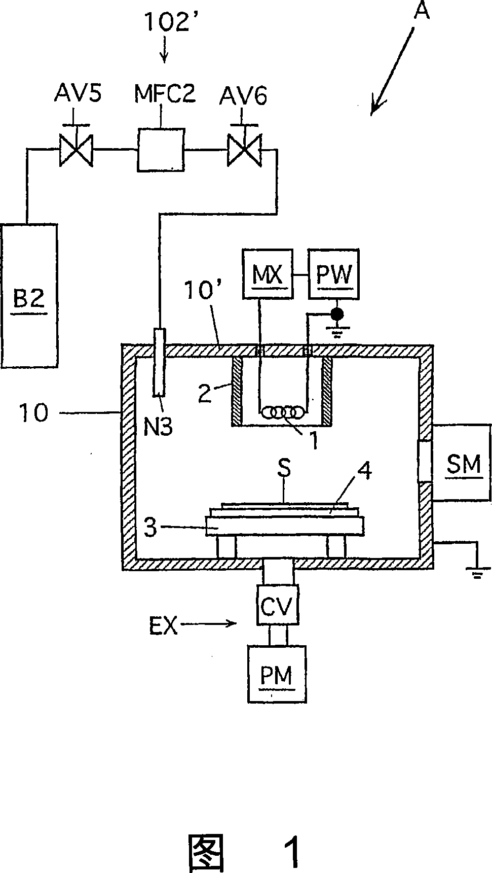
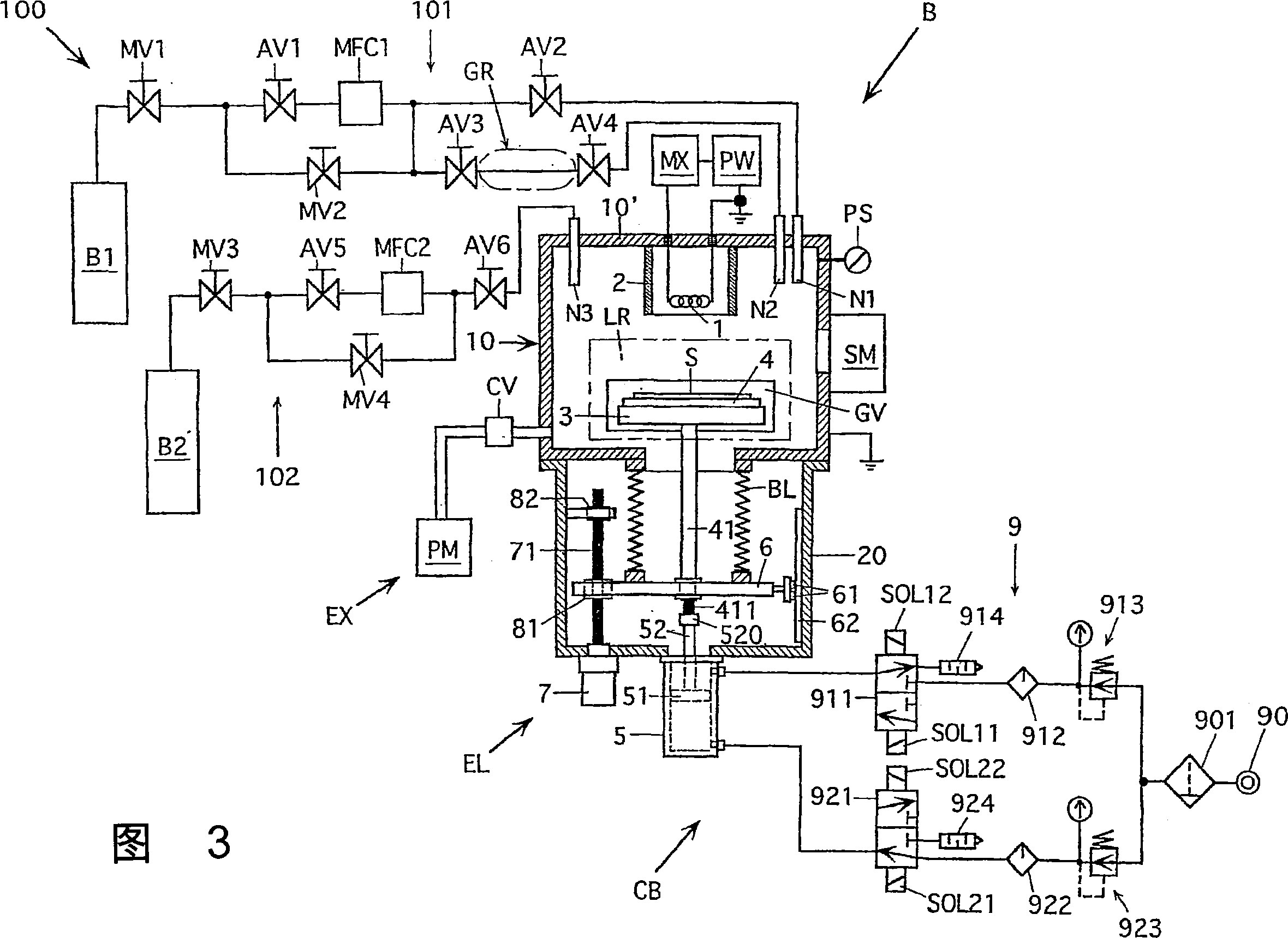
[0175] Film-forming conditions were as follows.

[0176] High frequency power: 60 MHz, 4000 watts

[0177] The silane gas (SiH 4 ) pressure and volume:

[0178] Pressure 0.07 Mbar

[0179] The amount can be selected from 100cc to 300cc, but in this embodiment it is 231cc

[0180] Silane gas supply amount of mass flow controller MFC1: 1 sccm

[0181] Mass flow controller MFC2 hydrogen supply: 150sccm

[0182] Film forming pressure: 0.67 bar (5 mTorr)

[0183] Film-forming chamber capacity: 1.5 cubic meters

[0184] Film substrate: non-alkali glass substrate

[0185] Film forming temperature: 400°C

[0186] Film thickness: 500 Angstroms

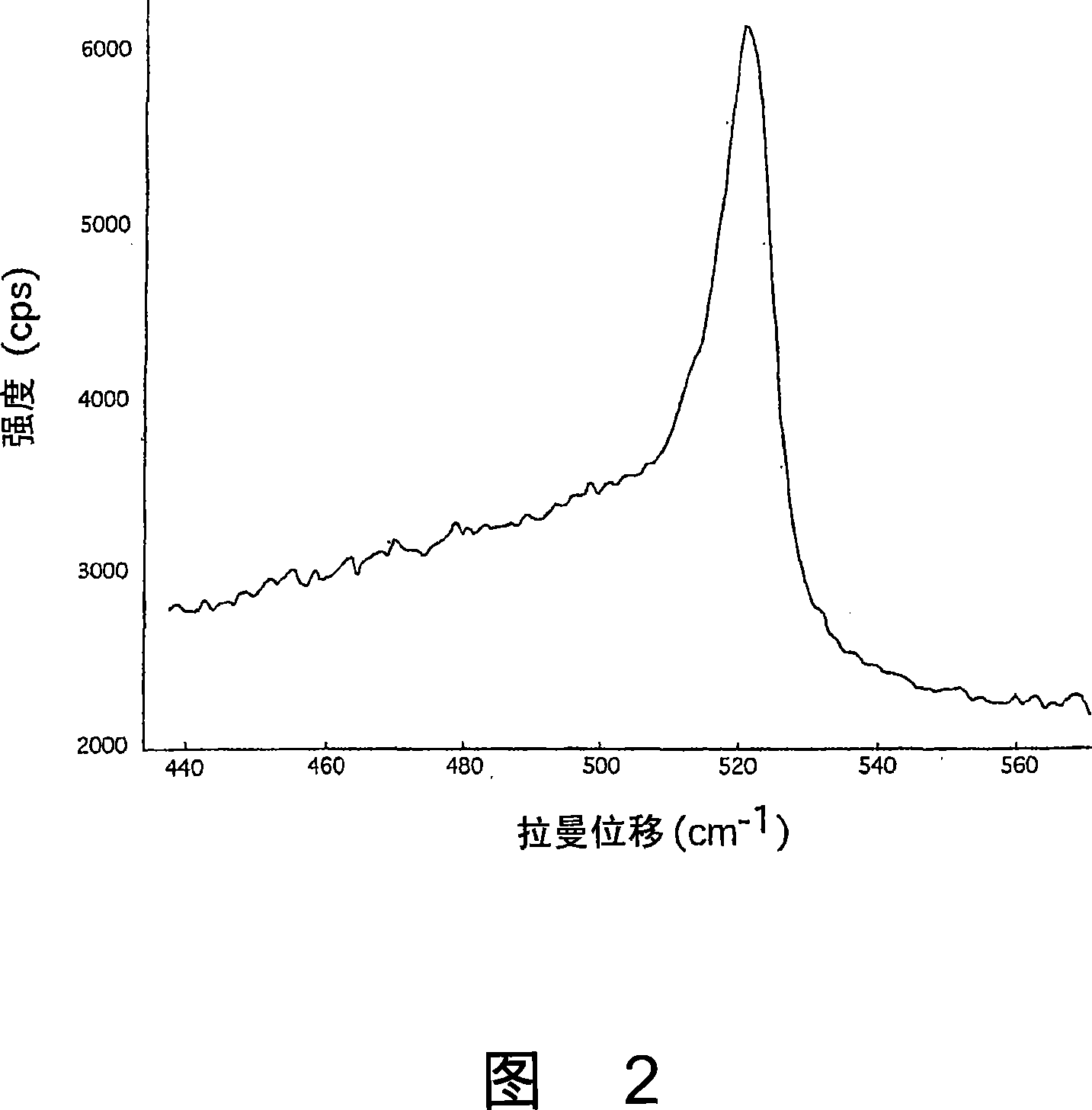
[0187] According to this condition, when a silicon film is formed on a substrate, and the UV reflective surface intensity on the substrate interface and the UV reflective surface intensity on the film surface are measured based on UV (ultraviolet) reflectance measurement, it is confirmed that the silicon film is at the film interface ...


PUM

PropertyMeasurementUnit
thicknessaaaaaaaaaa

Abstract

The invention discloses a silicon film forming device, comprising: a film forming chamber (10); a silicon sputtering target (2) arranged in the chamber; a hydrogen supply circuit (102 or 102') for supplying hydrogen to the chamber; and A high-frequency power application device (antenna (1, 1'), power supply (PW), etc.) that applies high-frequency power to the hydrogen gas supplied to the film forming chamber (10) to generate inductively coupled plasma, and uses the plasma to target ( 2) Perform chemical sputtering to form a silicon film on the substrate (S). Silane gas can also be used simultaneously. A gas storage unit (GR) may also be provided in the silane gas supply circuit (101). A desired silicon film can be formed inexpensively and at high speed at relatively low temperature.

Description

technical field [0001] The present invention relates to a silicon film forming device. Background technique [0002] Silicon films are used, for example, as materials for TFT (Thin Film Transistor) switches provided in pixels of liquid crystal display devices, and are used in the production of various integrated circuits, solar cells, and the like. It is also expected to be used as a non-volatile memory, a light-emitting element, and a photoactivator. [0003] As a silicon film forming method, various methods are known, for example, a method of forming an amorphous silicon film at a relatively low temperature by various CVD methods and PVD methods, and further performing, for example, 1000 steps of processing the amorphous silicon film formed in this way. ℃ heat treatment or heat treatment at 600 ℃ for a long time to form a crystalline silicon film, maintain the temperature of the substrate to be filmed at 600 ℃ to 700 ℃ and use CVD methods such as plasma CVD at low pressur...

Claims


Application Information

Patent Timeline
Patent Type & Authority Applications(China)
IPC IPC(8): C23C14/14C23C14/34H01L21/203C23C14/16H01J37/32
CPCC23C14/165C23C14/3471H01J37/321C23C14/34C23C14/548
Inventor 东名敦志高桥英治藤原将喜小寺隆志小野田正敏
Owner NISSIN ELECTRIC CO LTD
Why Eureka
Try Eureka