

Nitride-based semiconductor substrate and method of making the same
A technology of nitride system and manufacturing method, which is applied in semiconductor/solid-state device manufacturing, semiconductor devices, chemical instruments and methods, etc., can solve the problems such as the difficulty of offset between the substrate and the crystal lattice, and the obstacles of high-brightness LEDs. Achieve the effects of high conductivity, high reliability, high efficiency and high reliability
- Summary
- Abstract
- Description
- Claims
- Application Information
AI Technical Summary
Problems solved by technology
Method used
Image

Examples
Embodiment 1
[0064] (example of method using a)
[0065] Fig. 4 shows an example of the HVPE reactor used in this example.
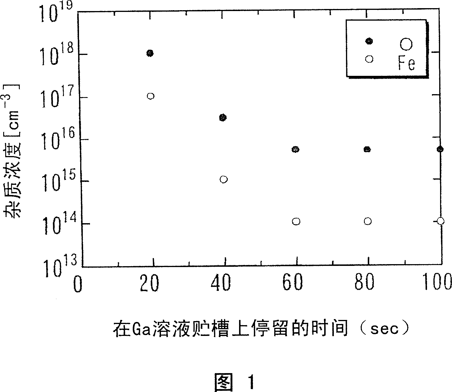
[0066] This HVPE reaction furnace 10 is a hot-wall type in which a heater 2 is installed on the outside of a horizontally long quartz reaction tube 1 to heat it. 3 gas NH 3 An introduction pipe 3, an HCl introduction pipe 4 for introducing HCl gas for forming GaCl as a group III raw material, and a doping pipe 5 for introducing a dopant gas for controlling conductivity. In addition, the diameter of the HCl introduction pipe 4 is enlarged in the middle to form a Ga melt storage tank 6, which can accommodate Ga melt 7. On the other hand, on the right side (downstream side) of the figure of the quartz reaction tube 1, there is provided a substrate holder 9 on which an underlying substrate 8 is disposed, and is freely rotatable and movable.
[0067] When using the HVPE reactor 10 to grow GaN, first 3 Introductory tube 3 introduces NH as a V-group raw material 3 As f...
Embodiment 2
[0073] (Example of method using a+b+c)
[0074] According to the steps shown in FIG. 5, a GaN free-standing substrate was produced.
[0075] First, a sapphire substrate 11(a) having a diameter of 2 inches is prepared as an underlying substrate, and a GaN film 12(b) having a thickness of 300 nm is formed on the sapphire substrate 11 by the MOVPE method. After (c) a Ti film 13 with a thickness of 20 nm was vacuum-evaporated thereon, in H 2 and NH 3 mixed atmosphere (H 2 The heat treatment was performed at 1000° C. for 30 minutes at a gas partial pressure of 80 kPa. After heat treatment, the Ti film 13 on the surface of the substrate is nitrided, and at the same time, due to the agglutination, it becomes porous TiN14 (d) with many micropores of tens of microns.
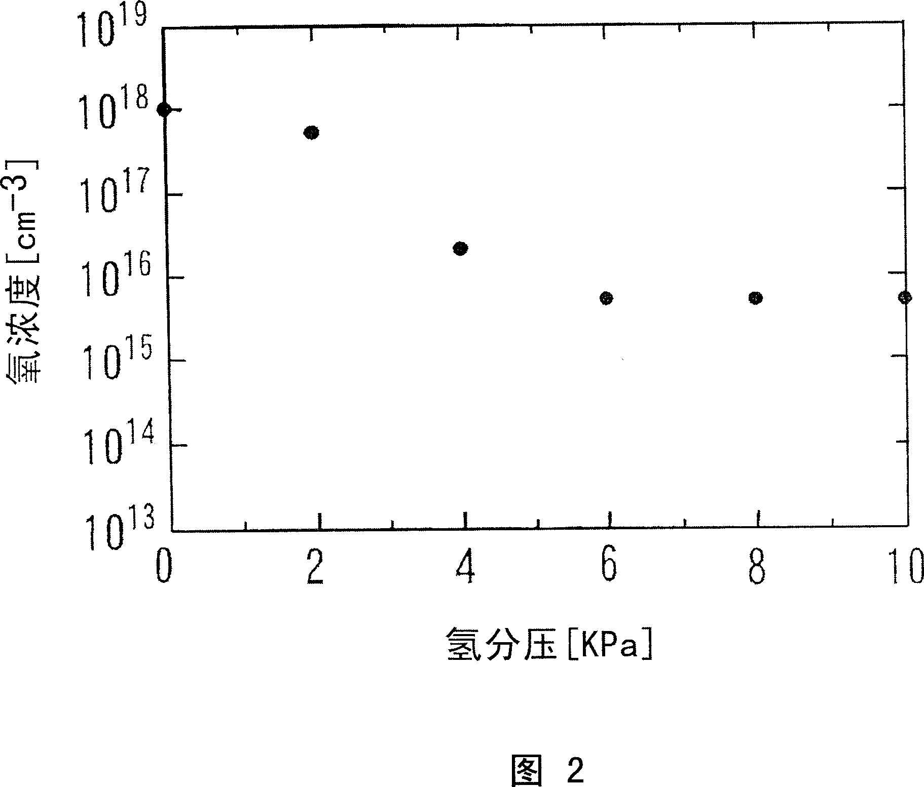
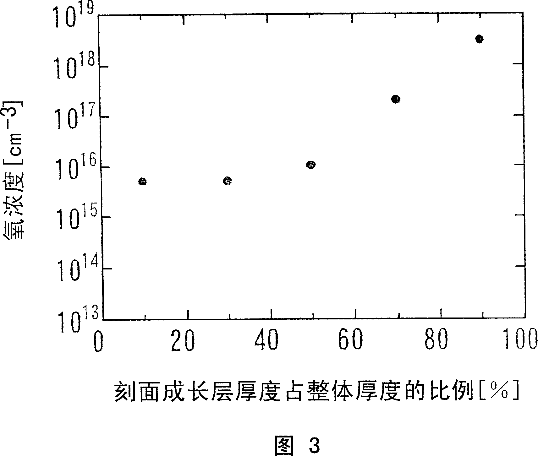
[0076] This was placed in the HVPE furnace shown in FIG. 4 to grow a GaN thick film 17 with a thickness of 500 μm. At this time, adjust the H 2 The flow rate of the carrier gas was such that the residence time of t...
experiment example
[0088] Using the GaN free-standing substrates obtained in Example 2 and the prior art example, LEDs having the same structure were fabricated. Both drive voltages were good at about 3.8V when energized at 20mA. However, as a result of comparing the light output, the LED produced on the GaN free-standing substrate obtained in Example 2 was about 30% larger. The reason for this is considered to be that the GaN free-standing substrate of Example 2 has high transparency, and light generated in the active layer is efficiently emitted.
PUM
| Property | Measurement | Unit |
|---|---|---|
| diameter | aaaaa | aaaaa |
| dislocation density | aaaaa | aaaaa |
| absorptance | aaaaa | aaaaa |
Abstract
Description
Claims
Application Information