
Method for manufacturing niobate-system ferroelectric thin-film device

a technology of ferroelectric thin film and niobate, which is applied in the direction of vacuum evaporation coating, coating, sputtering coating, etc., to achieve the effects of low manufacturing cost, high dimensional accuracy and low cos

Active Publication Date: 2019-02-05
SUMITOMO CHEM CO LTD +1
View PDF33 Cites 2 Cited by
  • Summary
  • Abstract
  • Description
  • Claims
  • Application Information

AI Technical Summary

Benefits of technology

The technical effect of this patent text is that it provides a solution for improving the accuracy and efficiency of a robot's movement and positioning in a complex environment with obstacles and uneven surfaces. This is achieved through a combination of sensors, cameras, and artificial intelligence techniques that help the robot identify and avoid obstacles, and accurately position itself in relation to its surroundings.

Problems solved by technology

However, because there are currently no suitable commercially available alternative pyroelectric or piezoelectric materials, PZTs are exempt from the RoHS directive (the directive on the restriction of the use of specified hazardous substances in electrical and electronic equipment enforced by the European Union and Council of Europe).

Method used


Image

  • Method for manufacturing niobate-system ferroelectric thin-film device
  • Method for manufacturing niobate-system ferroelectric thin-film device
  • Method for manufacturing niobate-system ferroelectric thin-film device

Examples


examples

[0070]The present invention will be described more specifically below by way of examples. However, the invention is not limited to the specific examples below.

[0071]Examination 1

[0072][Potassium Sodium Niobate (KNN) Thin Film Device]

[0073](Fabrication of KNN Thin Film-On-Substrate)

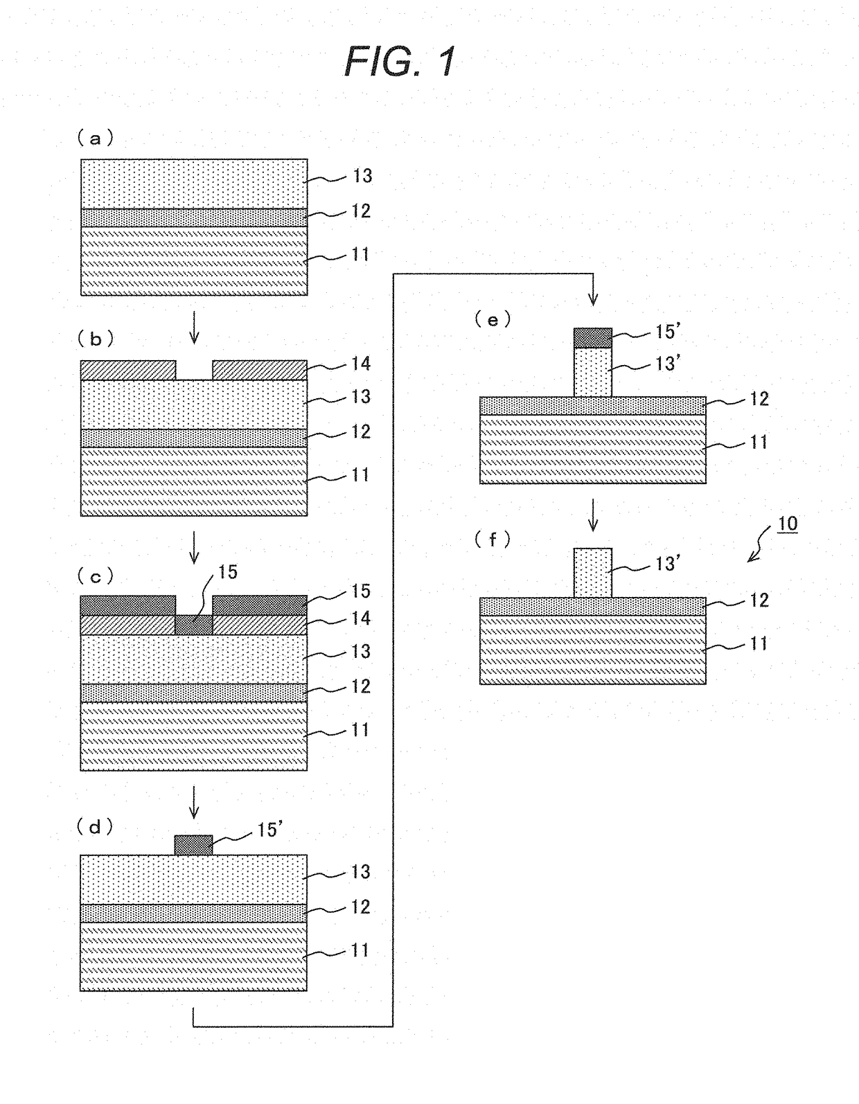
[0074]The KNN thin film-on-substrate 10 was fabricated according to the manufacturing steps illustrated in FIG. 1. A 4-inch (100) Si wafer with thermal oxide (Si wafer thickness of 0.525 mm; oxide thickness of 200 nm) was used as the substrate 11.

[0075]First, a 2.2-nm thick Ti layer was formed on the substrate 11 by RF magnetron sputtering in order to enhance adhesion between the substrate 11 and the lower electrode film 12. Next, the lower electrode film 12 was formed by forming a 205-nm thick Pt layer on the Ti layer by RF magnetron sputtering (see FIG. 1(a)). The sputtering conditions for the Ti adhesive layer and Pt lower electrode film 12 were as follows: targets of pure Ti (for the Ti layer) and pure...


PUM

PropertyMeasurementUnit
temperatureaaaaaaaaaa
Raaaaaaaaaaa

Abstract

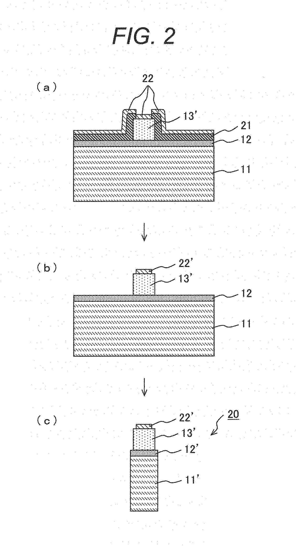
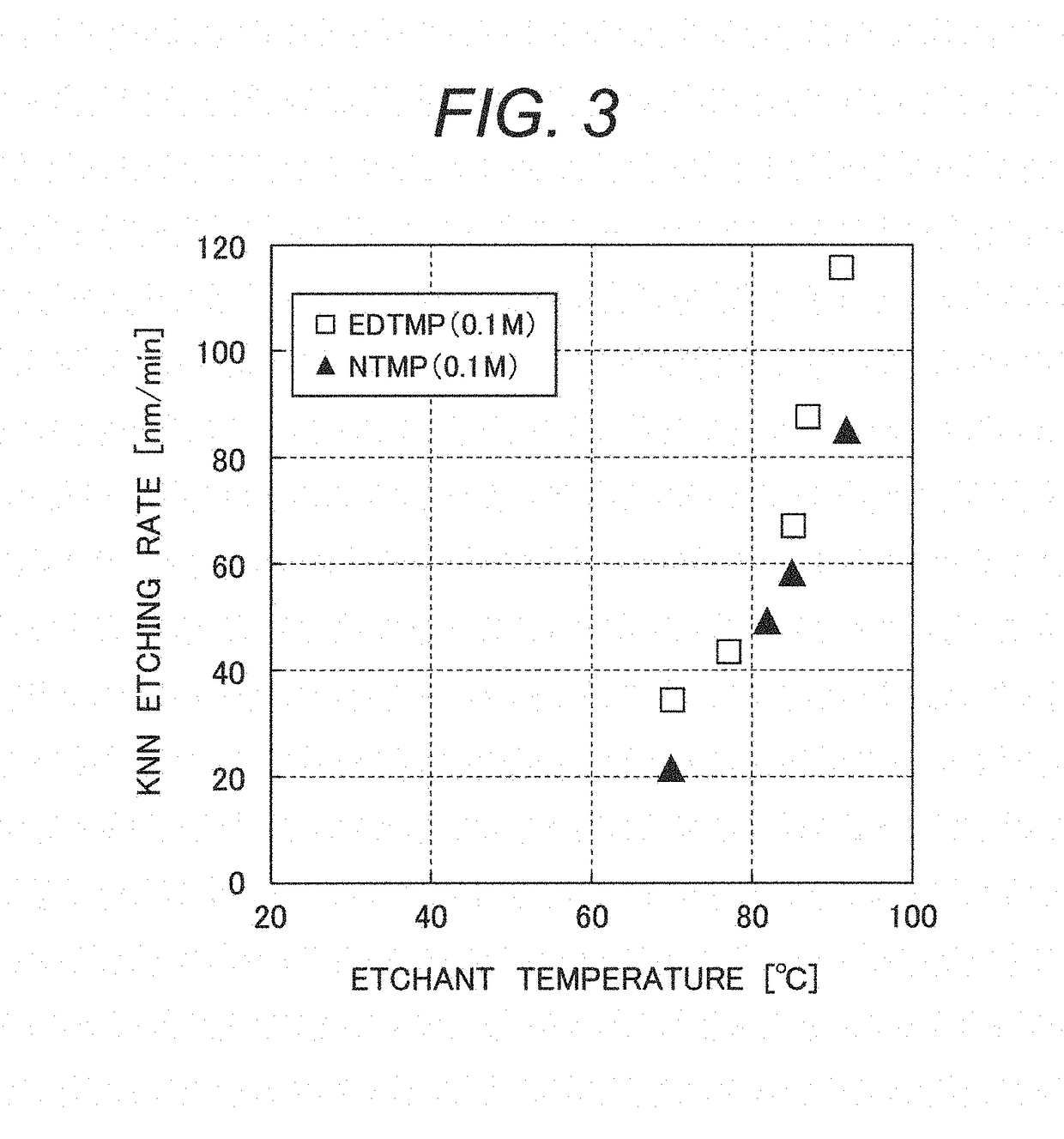
This method for manufacturing a lead-free niobate-system ferroelectric thin film device includes: a lower electrode film formation step of forming a lower electrode film on a substrate; a ferroelectric thin film formation step of forming a niobate-system ferroelectric thin film on the lower electrode film; an etch mask pattern formation step of forming an etch mask in a desired pattern on the niobate-system ferroelectric thin film; and a ferroelectric thin film etching step of shaping the niobate-system ferroelectric thin film into a desired fine pattern by wet etching using an etchant comprising: a predetermined chelating agent including at least one selected from EDTMP, NTMP, CyDTA, HEDP, GBMP, DTPMP, and citric acid; an aqueous alkaline solution containing an aqueous ammonia solution; and an aqueous hydrogen peroxide solution.

Description

TECHNICAL FIELD OF THE INVENTION[0001]The present invention relates to technologies regarding ferroelectric thin film devices and particularly to methods for manufacturing lead-free niobate-system ferroelectric thin film devices.DESCRIPTION OF BACKGROUND ART[0002]Ferroelectrics are very attractive substances because of their peculiar characteristics (such as very high relative permittivity, and good pyroelectric, piezoelectric and ferroelectric properties). So, various devices (such as ceramic multilayer capacitors, pyroelectric devices, piezoelectric devices and ferroelectric memories) have been developed and put into use utilizing such peculiar properties. Typical ferroelectrics are perovskite materials such as barium titanate (BaTiO3) and lead zirconate titanate (Pb(Zr1-xTix)O3, PZT). Of these, lead zirconate titanates (PZTs) provide relatively excellent polarization and piezoelectric properties and are therefore most widely used.[0003]Lead-containing PZTs are specified hazardous...

Claims


Application Information

Patent Timeline
Patent Type & Authority Patents(United States)
IPC IPC(8): H01L41/316H01L41/332H01L41/187H01L41/113C23C14/08H01L21/308C23C14/34
CPCH01L41/316C23C14/08C23C14/34H01L41/332H01L41/113H01L41/187H01L41/1873H01L21/308H10N30/8542H10N30/082H10N30/076H10N30/30H10N30/853
Inventor HORIKIRI, FUMIMASASHIBATA, KENJIWATANABE, KAZUTOSHISUENAGA, KAZUFUMINOGUCHI, MASAKIKUROIWA, KENJI
Owner SUMITOMO CHEM CO LTD
Learn More