Receiver for receiving differential signal, IC including receiver, and display device

a technology for receiving differential signals and display devices, which is applied in static indicating devices, single-ended push-pull amplifiers, instruments, etc., can solve the problems of reducing display quality, increasing the number of wirings, and increasing power consumption, and achieve high input/output linearity

Inactive Publication Date: 2019-03-05
SEMICON ENERGY LAB CO LTD
View PDF24 Cites 2 Cited by
  • Summary
  • Abstract
  • Description
  • Claims
  • Application Information

AI Technical Summary

Benefits of technology

[0089]In the receiver 100, the differential pair 111 receives the differential signals which are transmitted from the transmitter 105. Thus, the transistors NM1 and NM2 can be MV devices so as to have a high withstand voltage, and the other transistors can be LV devices, which have more excellent frequency characteristics. Therefore, the operating frequency of the receiver 100 can be increased, and the transmission delay time thereof can be reduced. No need to provide a level shifter in the output stage of the receiver 100 significantly contributes to the increase in the operating frequency and the reduction in the transmission delay time. The receiver 100 mostly constituted by LV devices can have advantageous effects such as reductions in circuit area and power consumption.
[0090]The amplifier circuits 110 and 120 can each be a single-power-supply amplifier circuit. The amplifier circuit 110 preferably has high input / output linearity. The amplifier circuit 120 preferably has rail-to-rail output capability.
[0091]Some specific circuit configuration examples of receivers are described below.<<Receiver 140>>
[0092]FIG. 2 illustrates a configuration example of a receiver. The receiver 140 includes amplifier circuits 150 and 160 and terminals INP, INN, OUT, VH, VL, NCAS, PCAS, NBIAS, and PBIAS.
[0093]The amplifier circuit 150 is a folded cascode operational amplifier. The amplifier circuit 160 is a buffer operational amplifier.
[0094]The terminals INP and INN are input terminals for differential signals, and the terminal OUT is an output terminal for a single-ended signal. The terminal VH is an input terminal for a power supply voltage Vddd, and the terminal VL is an input terminal for a power supply voltage Vssd. Each of the terminals NCAS, PCAS, NBIAS, and PBIAS is an input terminal for a bias voltage. Voltages Vcs1, Vcs2, Vbs1, and Vbs2 are input to the terminals NCAS, PCAS, NBIAS, and PBIAS, respectively.<Amplifier Circuit 150>

Problems solved by technology

An increase in resolution of a display device causes an increase in the number of wirings for transmitting an image signal to the display device, an increase in power consumption, or the like in many cases.
In addition, the high-resolution display device is likely to be influenced by noise, for example, electromagnetic interference (EMI), which often reduces display quality.

Method used


Image

  • Receiver for receiving differential signal, IC including receiver, and display device
  • Receiver for receiving differential signal, IC including receiver, and display device
  • Receiver for receiving differential signal, IC including receiver, and display device

Examples


embodiment 1

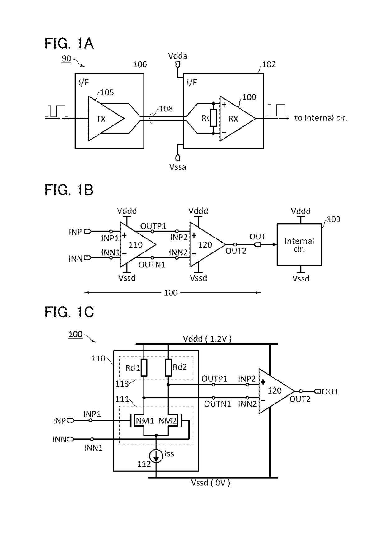
[0066]FIG. 1A illustrates an overview of a system for transmitting a digital signal using a differential signal (a differential transmission system). An example in which LVDS is a differential transmission method is described here. In a differential transmission system 90 illustrated in FIG. 1A, an interface (I / F) circuit 102 at the receiving end includes a receiver (RX) 100, and an interface circuit 106 at the transmitting end includes a transmitter (TX) 105. The transmitter 105 converts a single-ended signal into a differential signal. The differential signal is transmitted to the receiver 100 via a transmission medium 108.

[0067]The transmitter 105 has a function of converting a single-ended digital signal into a differential signal. The differential signal that is output from the transmitter 105 is input to the receiver 100 via the transmission medium 108. The transmission medium 108 includes two wirings. A resistor Rt is a termination resistor at the receiving end and has a resi...

configuration example 1

[0126]FIG. 8 illustrates a configuration example of an LVDS receiver IC with four input channels. An LVDS receiver IC 200 includes receivers 2101> to 2104>, a bias voltage generation circuit 212, a reference current generation circuit 213, a logic circuit 215, and pins RINP1 to RINP4, RINN1 to RINN4, ROT1 to ROT4, VH1, VL1, and CE.

[0127]The pins RINP1 to RINP4 and RINN1 to RINN4 are input pins for differential signals. In the LVDS receiver IC 200, a resistor for terminating the pin RINP1 and the pin RINN1 is provided. The other input pins for differential signals are also terminated similarly.

[0128]The pins ROT1 to ROT4 are output pins for single-ended signals. The pins VH1 and VL1 are input pins for power supply voltages; for example, the power supply voltage Vddd is input to the pin VH1 and a ground voltage (GND) is input to the pin VL1. The pin CE is an input pin for a chip enable signal.

[0129]The logic circuit 215 generates the signals STBE and STBEB based on the chip enable sig...

configuration example 2

[0131]FIG. 9 illustrates a configuration example of an LVDS receiver IC. An LVDS receiver IC 201 has four input channels and has a function of outputting a 32 (4×8) bit parallel data signal. The LVDS receiver IC 201 has a function of a deserializer. The LVDS receiver IC 201 includes receivers 2101> to 2105>, serial-parallel (S / P) converter circuits 2201> to 2204>, a phase locked loop (PLL) circuit 221, a bias voltage generation circuit 212, a reference current generation circuit 213, a logic circuit 215, and pins RINP1 to RINP4, RINN1 to RINN4, CKINP, CKINN, ROT1_1 to ROT1_8, ROT2_1 to ROT2_8, ROT3_1 to ROT3_8, ROT4_1 to ROT4_8, RCKO, VH1, VL1, and CE.

[0132]The LVDS receiver IC 201 includes four data lanes and one clock lane. Differential clock signals RCLK_P and RCLK_N are input to the clock lane from the pins CKINP and CKINN. The receiver 2105> converts the differential clock signals RCLK_P and RCLK_N into a single-ended clock signal. The PLL circuit 221 generates a clock signal C...


PUM


Abstract

The transmission delay time of a receiver for receiving a differential signal is reduced. A first amplifier circuit is provided in an input stage of the receiver, and a second amplifier circuit is provided in an output stage of the receiver. The first amplifier circuit is a differential input, differential output amplifier circuit. The second amplifier circuit is a differential input, single-ended output amplifier circuit. A first power supply voltage and a second power supply voltage are input as a high-level power supply voltage and a low-level power supply voltage to the first amplifier circuit and the second amplifier circuit, respectively. The withstand voltage of transistors of a differential pair of the first amplifier circuit is higher than the withstand voltage of another transistor included in the first amplifier circuit and a transistor included in the second amplifier circuit.

Description

TECHNICAL FIELD[0001]The specification, drawings, and claims of this application (hereinafter referred to as “this specification and the like”) relate to a semiconductor device, an electronic component, an electronic device, operating methods thereof, and manufacturing methods thereof. Examples of a technical field of one embodiment of the present invention include a semiconductor device, a memory device, a processing device, a switch circuit (e.g., a power switch and a wiring switch), a display device, a liquid crystal display device, a light-emitting device, a lighting device, a power storage device, an input device, an imaging device, driving methods thereof, and manufacturing methods thereof.BACKGROUND ART[0002](1) A differential transmission method is a method for transmitting data. As a typical differential transmission method, low-voltage differential signaling (LVDS) is known (see Non-Patent Documents 1 and 2). For example, Patent Document 1 discloses a technique that enable...

Claims


Application Information

Patent Timeline
Patent Type & Authority Patents(United States)
IPC IPC(8): G09G3/36H03F3/45H01L27/32G09G3/20G09G3/3275H03F3/68H03F3/195H03F3/30H01L27/12G09G5/02
CPCG09G3/2096G09G3/3648G09G3/3677G09G3/3688H01L27/3211H01L27/3244H03F3/195H03F3/3022H03F3/45183H03F3/45192H03F3/45219H03F3/45475H03F3/68G09G3/3275H03F2203/45652G09G5/026G09G2300/046G09G2300/0408G09G2300/0871G09G2310/0286G09G2310/0291G09G2320/0666G09G2330/06G09G2340/02G09G2360/121G09G2360/144G09G2360/18G09G2370/08G09G2370/14H01L27/1225H10K59/35H10K59/12
Inventor INOUE, HIROKITAKAHASHI, KEI
Owner SEMICON ENERGY LAB CO LTD
Why Eureka
Try Eureka