Deposition process based on stencil mask and application to the fabrication of tags supporting multi-functional traceable codes

a stencil mask and stencil technology, applied in the field of equipment for production, a production methodology and an architecture for tags, can solve the problems of species decomposition, difficult structure, no solution for chemical deposition techniques, etc., and achieve the effect of high refractive index and robust solution

Active Publication Date: 2019-05-07
3D OXIDES
View PDF9 Cites 3 Cited by
  • Summary
  • Abstract
  • Description
  • Claims
  • Application Information

AI Technical Summary

Benefits of technology

[0077]In order to achieve the above described combination, the invention provides the use of a mask, or a stencil mask, in combination with chemical precursors in vacuum with line of sight ballistic transport to deposit thin film materials, in preference of multifunctional materials. With the combination of such elements, high resolution patterns can be achieved, deposition on the mask can be avoided and complex combination (controlled gradients) of elements and properties within a structure can be produced with micrometric and sub-micrometric resolution.
[0091]In a further preferred embodiment the process further comprises providing a flow of a different chemical precursor, whereby the different chemical precursor differs from any chemical precursor of the plurality of chemical precursor beams, whereby the different chemical precursor has a higher decomposition temperature in comparison to a main precursor of the plurality of chemical precursors used to achieve a thin film, by blowing the further flow in a direction substantially tangential to the mask, thereby minimizing the impinging rate of the further flow on the substrate, but optimising the impinging rate of the further flow on the mask surface, the different chemical precursor being used to inhibit decomposition of the main precursor on the mask, but not on the substrate.
[0110]In a seventh aspect, the invention provides a tag displaying a partition of regions, one of the regions displaying uniform or graded properties taken amongst the list comprising at least thickness, colour, electrical conductivity, the properties being those of a material that are further modifiable by light irradiation or a chemical process to achieve a logo, a serial number or any distinctive additional feature that will contribute to enhance traceability, anti-forgery or cryptographic functionalities.
[0117]In a ninth aspect, the invention provides a book-cipher-like encrypting method based on material properties mapping, and comprising at least using at least two identical tags, one of which used as key-code, the security of the solutions being enhanced by the possibility to have a plurality of different and independent codes available in the tag and by the fact that the at least two identical tags are unique and cannot be forged.
[0119]In a further preferred embodiment of the packaging, the tag is embedded in polymer foils thereby enabling a more robust solution or directly melted into a material such as a glass bottle or different other transparent media as the tag multifunctional thin film material may withstand high temperatures and the thin film material has a high refractive index.

Problems solved by technology

These materials are usually physically hard and chemically inert which make them difficult to structure by standard technologies including mechanical machining or chemical etching steps, e.g., standard top-down approach, including ion beam structuring, electro beam writing or photo-lithography.
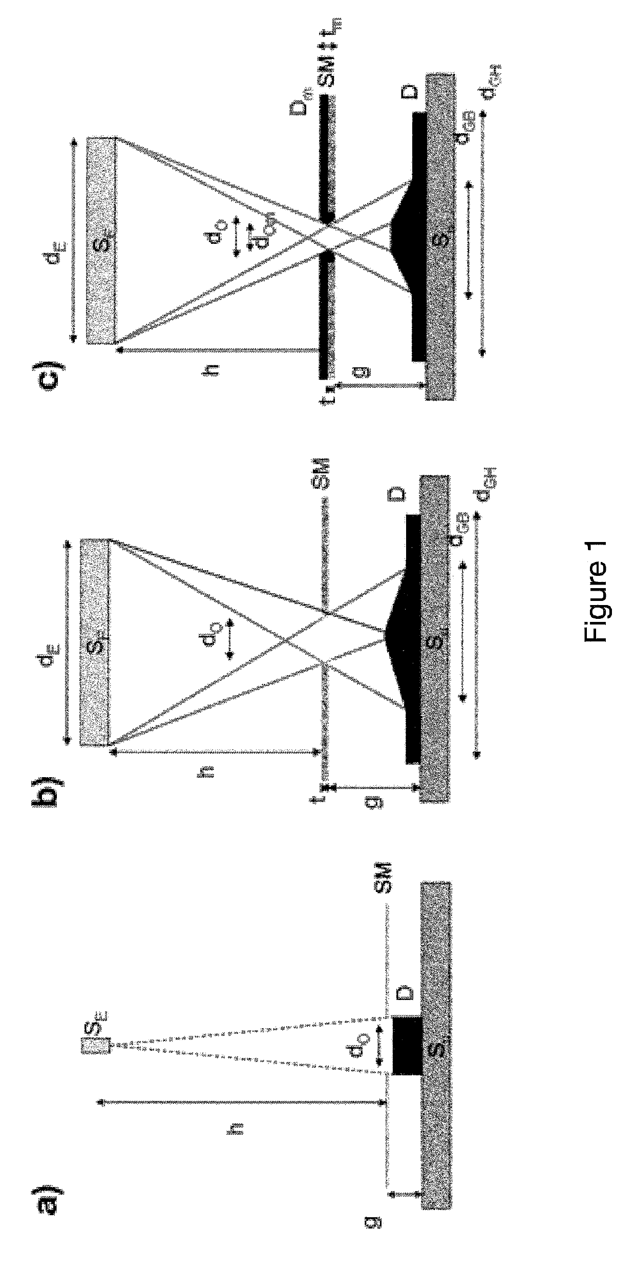
FIG. 1 presents some of the major problems associated with state of the art technology, which principally are [9] [10]:a) The blurring, which is a widening of the deposited pattern dimension compared to the stencil aperture size, due to the existing gap between the stencil and the substrate.
It is particularly problematic when deposited thickness is of the same order or higher than the aperture size in the case of nano-stencils.
This is no solution for a chemical deposition technique in which reactive species decompose due to thermal heating, and it does not work with non volatile species.
In addition, deposition may take place on the mask top and side (image c), leading to clogging, due a deposit Dm that affects the aperture dimension (reduced from dO to dOm) and mask thickness (increased from t to tm).
Forgery and counterfeiting are problematic that organised societies have had to fight since the very beginning.
Everyone is aware of counterfeited products such as luxury goods, e.g. watches, handbags, jewels, softwares, DVDs, CDs, etc., but the plague also extends to new products such as pharmaceuticals or toys, where the problem is no longer only economical, but also impacting people's health or even putting their lives at risk.
. . ), up to very complex collaborative clouds or networks.
The societal plague associated with the lack of security of such systems (with identity hacking, frauds, phishing scam, intrusion into privacy etc.
A further difficulty to overcome for an efficient technology is an economic one [38]: should it provide a product a totally unique, with an irreproducible signature, etc., there is no hope for its development if the tag price is higher than the likely loss of income through counterfeiting.
On one hand, naked eye reading is a quite subjective and time consuming solution at large scale and overt technology labels contain a very limited amount of information.
On the over hand, covert or machine readable technologies require expensive / poor-mobility readers
Two different printing approaches are today available, either based on sequential (or serial) printing or based on parallel printing techniques:the first methods of serial printing usually suffer from low resolution (thus containing low amount of information) or are time consuming and poorly cost efficient if higher resolution (with micro or nano dots resolution) is targeted (like for Plixel Printing).
The time required to print a highly resolved etiquette / tag / label is such that this method will never be suitable to address efficiently huge mass production of high security / high information density.
This is an intrinsic limit of such serial printing technologies.
However, the matrix production cost is usually very high and all the codes are identical, allowing neither flexibility nor variations on the tag (which is actually where the traceability and possibly enhanced security lays).
Again, if the core technology is cracked (the matrix is duplicated), all the security associated with this solution is gone.
In the first case, a pattern can be seen by naked eye, but does not provide any security mechanism.
When the ink secret composition is cracked, however, all the documents based on the technology can be forged.
Another drawback is related to recycling of such tags as mentioned in previous work (JPS62206695, JP2009276564) that very often contain rare or toxic elements.
Nevertheless, again these techniques suffer from most of the same intrinsic limits of printing methods with inks.
These methods are, however, very sensitive to the degradation of the object and identification of patterns can be quite time consuming.
Furthermore, they require complex and time-consuming reader solutions.
Several other inventions are disclosed for polymers or easily etchable or machined materials such as resins (US2008248266, JPH04118690), but with limited lifetime due to poor mechanical and chemical stability of the materials.
Materials with different refractive indexes are provided to achieve such an effect, leading either to limited effects or to very expensive assembly manufacturing.
These solutions are however quite expensive and complex to realize.
On one hand, such solution claims that the copper wires cannot be replicated, but the set-up is relatively simple and for sure cannot guarantee a huge number of different combinations.
On the other hand, the QR contains a very limited amount of information (black and white dots of low resolution).
Furthermore, no security is tied to these codes that can thus be easily copied and reproduced or moved to different objects.
The bar codes ease of reading is also their main weakness as anyone can forge or counterfeit them.
Furthermore, such marks contain only very limited amount of information and when large numbers of objects are to be tracked (over 1 billion), the system rapidly gets to its limits.
One solution is to further increase dot resolution or to add colour (JPS62206695, CN2448723), but this still yields intrinsic limits to security and anti-forgery issues.RFID (radio frequency identification)
. . These RFID tags offer high reliability without contact reading method, but readers and codes themselves are getting quite expensive and with a poor mobility.
However, these tags are quite expensive (15 cts for passive tags, 25 dollars for active tags [52]) and usually require bulky readers or energy supply.
Furthermore, a huge quantity of tags (above 1'000) within a reader will lead to confusion and misreading.
As a further disadvantage we can also quote that RFID, or other purely electronic systems, are usually providing poor security as tags can be moved from one product to another easily.
Finally, being a remote reading process, tracking of people wearing such tags on their products is a main limit to this technology as it disregards any privacy policy.
However, these solutions cannot be applied to objects.
Password-based systems furthermore have the weakness than when the password is cracked unlimited access is guaranteed.
Furthermore, the over-increasing number of required passwords leads to poorly safe methodology to generate and store such passwords at individual level.
More secure systems, involving hardware for PW generation, rely on additional manual time consuming endless password checks that are a real hurdle to the end-user and cannot manage a huge number of secured transactions in a timely manner.

Method used


Image

  • Deposition process based on stencil mask and application to the fabrication of tags supporting multi-functional traceable codes
  • Deposition process based on stencil mask and application to the fabrication of tags supporting multi-functional traceable codes
  • Deposition process based on stencil mask and application to the fabrication of tags supporting multi-functional traceable codes

Examples


Embodiment Construction

[0132]FIG. 3 describes the effect of the mask / substrate-to-be-covered gap to deposit 3D structures. Schemas a) and b) shows the deposit from two punctual sources PA and PB through a mask (SM) on a substrate Su through two different openings. Depending on the distance p between apertures, on dimension apertures d and on mask-subtrate gap g, the flows from the two sources can either remain separated (image a) or partially superimpose (image b) or almost fully superimpose. If precursors for different elements are used in the two sources, such deposition process allows obtaining in a single step separated deposits of different elements with different thicknesses, or co-deposition of different elements with varying chemical composition and thickness within the deposit or thin film structure.

[0133]Pictures c) and d) shows TiO2 deposit AFM profiles for the deposition from 10 neighbouring Ti precursor sources through a single triangular deposit for a substrate mask gap g of about 80 μm and ...


PUM

PropertyMeasurementUnit
thickaaaaaaaaaa
distanceaaaaaaaaaa
distanceaaaaaaaaaa

Abstract

A chemical gas phase deposition process comprises steps of providing a high vacuum chamber, and inside the high vacuum chamber: positioning a substrate surface; positioning a mask parallel to the substrate surface, whereby the mask comprises one or more openings; adjusting a gap of determined dimension between the substrate surface and the mask; and orienting a plurality of chemical precursor beams of at least one precursor species towards the mask with line of sight propagation, each of the plurality of chemical precursor beams being emitted from an independent punctual source, and molecules of the chemical precursor pass through the one or more mask openings to impinge onto the substrate surface for deposition thereon. At least a part of the chemical precursor molecules decompose on the substrate surface at a decomposition temperature. The process further comprises adjusting a temperature of the substrate surface greater or equal to the chemical precursor molecule decomposition temperature, thereby remaining greater than a mask temperature, and maintaining the mask temperature below the decomposition temperature, thereby causing a decomposition of the chemical precursor and a growth of a film on the substrate surface, but not on the mask; and heating the substrate surface using a heating device.

Description

CROSS REFERENCE TO RELATED APPLICATIONS[0001]The present application is a U.S. national stage application of PCT / IB2015 / 051983 filed on Mar. 18, 2015 designating the United States, and claims foreign priority to International patent application PCT / IB2014 / 000802 filed on Mar. 18, 2014, the contents of both documents being herewith incorporated by reference in their entirety.TECHNICAL FIELD[0002]The invention relates to an equipment for production, a methodology of production and an architecture for a tag. An additive manufacturing method and system for nano and micro 3D-printing of smart and multifunctional thin film materials is disclosed. Single step patterned thin film deposition with a vacuum chemical deposition process in conjunction with stencils masks with micro and nano aperture dimensions to achieve patterned multifunctional oxide thin film deposition is disclosed. Such a process would be applied in particular for one application, a tag device that enables simultaneous auth...

Claims


Application Information

Patent Timeline
Patent Type & Authority Patents(United States)
IPC IPC(8): C23C16/04B42D25/41B42D25/415B65D79/00G09F3/00C23C16/52B65C9/00C23C16/46C23C16/40
CPCC23C16/46C23C16/52G09F3/00C23C16/042C23C16/40B42D25/415B65C9/00B65D79/00B42D25/41C23C16/56B42D25/40G09F3/0297G09F3/0376
Inventor BENVENUTI, GIACOMOWAGNER, ESTELLESANDU, COSMIN
Owner 3D OXIDES
Why Eureka
Try Eureka