

Method for manufacturing silicon wafer
a manufacturing method and single crystal technology, applied in the direction of polycrystalline material growth, crystal growth process, after-treatment details, etc., can solve the problems of reducing the dielectric breakdown strength of an oxide film, adversely affecting the performance of the device, and affecting the characteristics of the device, so as to achieve less contamination or damage, high dielectric breakdown strength, and high device characteristics
Active Publication Date: 2019-05-21
SHIN-ETSU HANDOTAI CO LTD
View PDF28 Cites 0 Cited by
- Summary
- Abstract
- Description
- Claims
- Application Information
AI Technical Summary
Benefits of technology
This approach results in a silicon wafer with high dielectric breakdown strength and densely formed BMDs in the bulk, enhancing device reliability and preventing contamination, while avoiding slip dislocations and maintaining high wafer quality.
Problems solved by technology
It has been revealed that there are also microdefects (which will be referred to as grown-in defects hereinafter) which are formed other than OSFs during crystal growth and adversely affect device performance.
When the grown-in defects which are present in the V-Rich region, the OSF region and the I-Rich region appear on a wafer surface, they adversely affect device characteristics, for example, they decrease dielectric breakdown strength of an oxide film in a case where an MOS (Metal Oxide Semiconductor) structure of a device is formed, and hence it is desired that such defects are not present in a wafer surface layer.
It is known that, when this BMD is present in a bulk other than a device active region, it is effective since it functions as a gettering site to capture a metal impurity mixed during the device process, but it adversely affects the device characteristics such as junction leakage when it is produced on a silicon wafer surface which is the device active region.
Consequently, Va is non-uniformly distributed in a bulk.
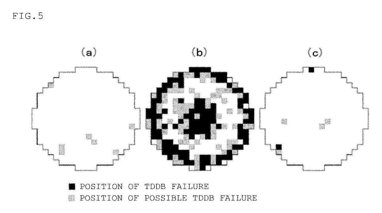
However, when a TDDB (Time Dependent Dielectric Breakdown) characteristic which is an aged breakdown characteristic representing long-term reliability of an oxide film is measured after a silicon wafer whose entire plane consists of an N region is prepared and the RTA treatment is performed, in an Nv region of the silicon wafer, a TZDB (Time Zero Dielectric Breakdown) characteristic which is one of oxide film reliabilities is hardly lowered, but there is a flaw that the TDDB characteristic is lowered.
However, since a difference in temperature between a pin which supports a wafer in an RTA treatment apparatus and the silicon wafer is considerable, strong stress is produced in a section around the pin, and there is a flaw that slip dislocations are generated.
However, according to such a method, since the back surface of the wafer must be brought into contact with the heat sink, there is a problem that a contact portion is apt to be damaged or contaminated and contamination possibly spreads from a member of the heat sink.
Method used
View moreImage
Smart ImageViewing Examples

Examples
examples
[0100]The present invention will now be more specifically described hereinafter with reference to an example and comparative examples, but the present invention is not restricted these examples.
[0101]A silicon wafer to be treated in which an Nv region and an Ni region are mixed was prepared, and Example and Comparative Examples 1 and 2 described below were carried out.
[0102]A conductivity type, a resistivity, oxygen concentration, a diameter, and a crystal axis orientation of the silicon wafer are follows.[0103]Conductivity type: P type[0104]Resistivity: 17 to 20 Ω·cm[0105]Oxygen concentration: 13 to 14 ppma (JEITA)[0106]Diameter: 300 mm[0107]Crystal axis orientation:
Login to View More PUM
| Property | Measurement | Unit |
|---|---|---|
| temperature | aaaaa | aaaaa |
| temperature | aaaaa | aaaaa |
| melting point | aaaaa | aaaaa |
Abstract
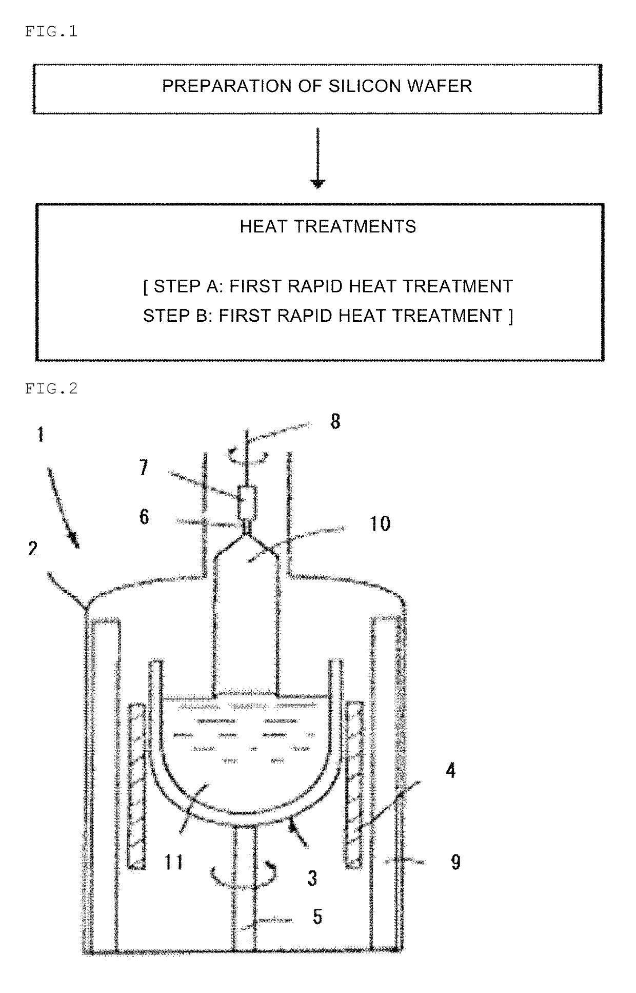
A method for manufacturing a silicon wafer having a denuded zone in a surface layer by performing a heat treatment to a silicon wafer, including: a step A, performing a first rapid heat treatment of 0.01 msec or more and 100 msec or less to an upper surface layer alone of the silicon wafer to be treated at 1300° C. or more and a silicon melting point or less by using a first heat source which heats the silicon wafer to be treated from above; and a step B, holding the silicon wafer to be treated at 1100° C. or more and less than 1300° C. for one second or more and 100 seconds or less by a second rapid heat treatment using a second heat source which heats the silicon wafer to be heated, and decreasing the temperature at a falling rate of 30° C. / sec or more and 150° C. / sec or less.
Description
TECHNICAL FIELD[0001]The present invention relates to a method for manufacturing a silicon single crystal wafer which provides high dielectric breakdown strength of an oxide film and enables highly densely forming oxide precipitates in the wafer.BACKGROUND ART[0002]A silicon single crystal wafer (which will be also referred to as a silicon wafer hereinafter) which can be a material of a semiconductor device can be generally fabricated by growing a silicon single crystal by a Czochralski method (which will be also referred to as a CZ method hereinafter) and performing a machining process such as cutting or polishing to the obtained silicon single crystal.[0003]In the silicon single crystal grown by the CZ method in this manner, oxidation induced stacking faults called OSFs (Oxidation induced Stacking Faults), which are annularly produced when the silicon single crystal is subjected to a thermal oxidation treatment (for example, 1100° C. for 2 hours), may be generated. It has been rev...
Claims
Login to View More Application Information
Patent Timeline
 Patent Type & AuthorityPatents(United States)
IPC IPC(8): H01L21/322C30B33/12H01L21/26C30B33/02C30B15/00C30B29/06
CPCH01L21/3225C30B15/00C30B29/06H01L21/322C30B33/12H01L21/26C30B33/02H01L21/324
InventorSUZUKI, KATSUYOSHITAKENO, HIROSHIEBARA, KOJI
OwnerSHIN-ETSU HANDOTAI CO LTD