Variable coding method for realizing chip reuse and communication terminal therefor

a technology of chip reuse and communication terminal, applied in logic circuits using specific components, logic circuits using semiconductor devices, pulse techniques, etc., can solve the problems of increasing the development cost of the integrated circuit system, moore's law gradually moving toward the limit, and putting chips into production

Active Publication Date: 2019-06-11
VANCHIP TIANJIN TECH
View PDF8 Cites 2 Cited by
  • Summary
  • Abstract
  • Description
  • Claims
  • Application Information

AI Technical Summary

Benefits of technology

[0024]The variable coding method provided by the present invention can use two or more identical integrated circuit chips to realize different logic control functions, thereby simplifying the types of chips for realizing system functions, and greatly lowering the development cost of the integrated circuit system and the management complexity of the mass production supply chain.

Problems solved by technology

However, as the process dimension is further reduced, Moore's Law is gradually moving toward the limit.
Since the cost of putting a chip into production is very high (its main cost is the cost of photolithography), this leads to an increase in the development cost of the integrated circuit system.
However, the existing component reusable technology still has many defects such as limited application scope, difficulty in solving the anti-interference problem, and the like.

Method used


Image

  • Variable coding method for realizing chip reuse and communication terminal therefor
  • Variable coding method for realizing chip reuse and communication terminal therefor
  • Variable coding method for realizing chip reuse and communication terminal therefor

Examples


embodiment 1

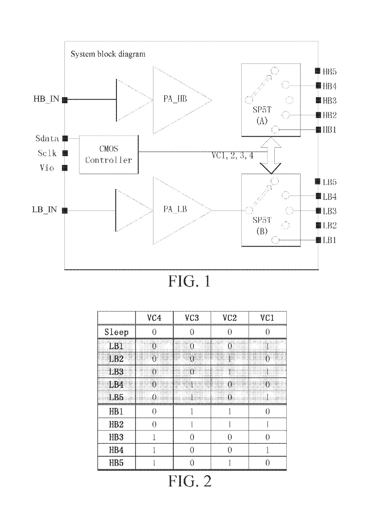
[0039]FIG. 1 is a system block diagram of an RF power amplifier (PA) and an RF switch module used by a certain communication terminal. In the drawing, the RF front end uses two single-pole five-throw (SPST) RF switch chips. The operating principles of the RF switch chips are the same, and the source (CMOS Controller) of the logic input signals VC1-VC4 used to control the RF switch chips is also the same. However, since the integrated circuit system requires that the two RF switch chips each perform the work of switching RF signals of different bands (for example, high band and low band), at the system level, they are two integrated circuit chips that are irreplaceable and must coexist, however, the only difference between them is that their control logic truth tables are different.

[0040]As shown in FIG. 2, the control logic truth table defined by the integrated circuit system for the high band (HB) and the low band (LB) is different. In order to realize these functions, two differen...

embodiment 2

[0047]As shown in FIG. 7, in another embodiment of the present invention, the input end of the logic control signal Vctrl is pulled up to the power (VDD) end by a slightly larger resistor in the circuit design stage, so that the Vctrl pin of the RF switch chip A applied to high band (HB) RF signals can be suspended (it is not necessary to connect it to a fixed level in the packaging stage.). At this time, it is only necessary to connect the Vctrl pin of the RF switch chip B to the ground (GND) end, thereby reducing the wire bonding to the power (VDD) end.

[0048]The pull-up resistor referred to here is not limited to a passive thin film resistor, but may also be various types of transistors in an appropriate bias state. The choice of its resistance or equivalent resistance needs to be considered in a compromise: it is necessary to consider the strength of the pull-up to resist interference, which requires that the pull-up resistor cannot be too large; and it is also necessary to consi...

embodiment 3

[0049]As shown in FIG. 8, in still another embodiment of the present invention, the input end of the logic control signal Vctrl is pulled down to the ground (GND) end by a slightly larger resistor, so that the Vctrl pin of the RF switch chip B applied to low band (LB) RF signals can be suspended (it is not necessary to connect it to a fixed level in the packaging stage.). At this time, it is only necessary to connect the Vctrl pin of the RF switch chip A to the power (VDD) end, thereby reducing the wire bonding to the ground (GND) end.

[0050]The pull-down resistor referred to here is not limited to a passive thin film resistor, but may also be various types of transistors in an appropriate bias state. The choice of its resistance or equivalent resistance needs to be considered in a compromise: it is necessary to consider the strength of the pull-down to resist interference, which requires that the pull-down resistor cannot be too large; and it is also necessary to consider that when ...


PUM


Abstract

Disclosed is a variable coding method for realizing chip reuse, comprising the following steps: using at least two identical integrated circuit chips, wherein each integrated circuit chip executes different control logic truth tables according to different gating signals; introducing at least one logical control signal as a gating signal; and controlling the logical control signal, so that each integrated circuit chip respectively executes a corresponding control logic truth table. Also disclosed is a communication terminal using the variable coding method for realizing chip reuse. Two or more completely identical integrated circuit chips can be used to realize different logical control functions, thereby simplifying the type of a chip for realizing a system function, and greatly reducing the development costs of an integrated circuit system and the management complexity of a mass production supply chain.

Description

RELATED APPLICATIONS[0001]This application is a National Phase of PCT Patent Application No. PCT / CN2016 / 108174 having International filing date of Nov. 30, 2016, which claims the benefit of priority of Chinese Patent Application No. 201510872771.4 filed on Dec. 1, 2015. The contents of the above applications are all incorporated by reference as if fully set forth herein in their entirety.FIELD AND BACKGROUND OF THE INVENTION[0002]The present invention relates to a variable coding method for realizing chip reuse, and further relates to a communication terminal for realizing chip reuse by using the variable coding method, belonging to the technical field of integrated circuits.[0003]The pursuit of miniaturization, multi-functionality, low cost, and low power consumption for electronic products is endless, which makes process improvement and system integration become the two major trends in the semiconductor industry. At present, the wafer manufacturing industry, which focuses on proce...

Claims


Application Information

Patent Timeline
Patent Type & Authority Patents(United States)
IPC IPC(8): H03K19/00H03K19/08H03K19/003H03K19/21H04B14/00
CPCH03K19/0002H03K19/00307H04B14/00H03K19/212H03K19/08
Inventor LIN, SHENG
Owner VANCHIP TIANJIN TECH
Why Eureka
Try Eureka