Manufacturing method of flexible TFT backplane and flexible TFT backplane

a manufacturing method and technology applied in the field of display techniques, can solve the problems that the base substrate used in the manufacturing method of flexible tft backplane can generally only tolerate low temperatures, and achieve the effects of reducing production costs, excellent conductivity, and saving production costs

Active Publication Date: 2020-05-26
SHENZHEN CHINA STAR OPTOELECTRONICS SEMICON DISPLAY TECH CO LTD
View PDF7 Cites 22 Cited by
  • Summary
  • Abstract
  • Description
  • Claims
  • Application Information

AI Technical Summary

Benefits of technology

[0007]The object of the present invention is to provide a manufacturing method of TFT backplane, able to be manufactured at a lower temperature and without limitation on the material of flexible base substrate, as well as, improving the electron mobility of the active layer of the TFT.
[0008]Another object of the present invention is to provide a flexible TFT backplane, with high electron mobility of the active layer of the TFT, good strength and flexibility.
[0056]The present invention provides the following advantages: the manufacturing method of flexible TFT backplane provided by the present invention uses a mixed solution of carbon nanotubes and a metal oxide to prepare an active layer of a TFT, and the temperature of the manufacturing is lower and will not cause damage to the flexible base substrate, and hence the material of the flexible base substrate is not restricted. The use of the vacuum equipment can be reduced to save production cost. The carbon nanotubes have excellent conductivity, and the mixture with the metal oxide as the active layer of the TFT can significantly improve the electron mobility. In addition, buffer layer made by the manufacturing method has a silicon nitride film as the lowest layer in contact with the flexible base substrate, which can make the good adhesion between the buffer layer and the flexible base substrate. The topmost layer of the buffer layer is an aluminum oxide film, which enables the buffer layer to have better resistance to water and vapor. The flexible TFT backplane provided by the present invention uses a mixed film of carbon nanotubes and metal oxides as an active layer of the TFT, which can significantly improve the electron mobility. The carbon nanotubes improve the strength and the flexibility of the active layer of the TFT and more suitable for fabricating a flexible display device. In addition, the buffer layer has a silicon nitride film as the lowest layer in contact with the flexible base substrate, which can make the good adhesion between the buffer layer and the flexible base substrate. The topmost layer of the buffer layer is an aluminum oxide film, which enables the buffer layer to have better resistance to water and vapor.

Problems solved by technology

In the current technology, the base substrate used in the manufacturing method of the flexible TFT backplane can generally only tolerate low temperatures.

Method used


Image

  • Manufacturing method of flexible TFT backplane and flexible TFT backplane
  • Manufacturing method of flexible TFT backplane and flexible TFT backplane
  • Manufacturing method of flexible TFT backplane and flexible TFT backplane

Examples


Embodiment Construction

[0070]To further illustrate the technical means taken by the present invention and resulted effects, the following detailed description is made in conjunction with the preferred embodiments of the present invention and the accompanying drawings.

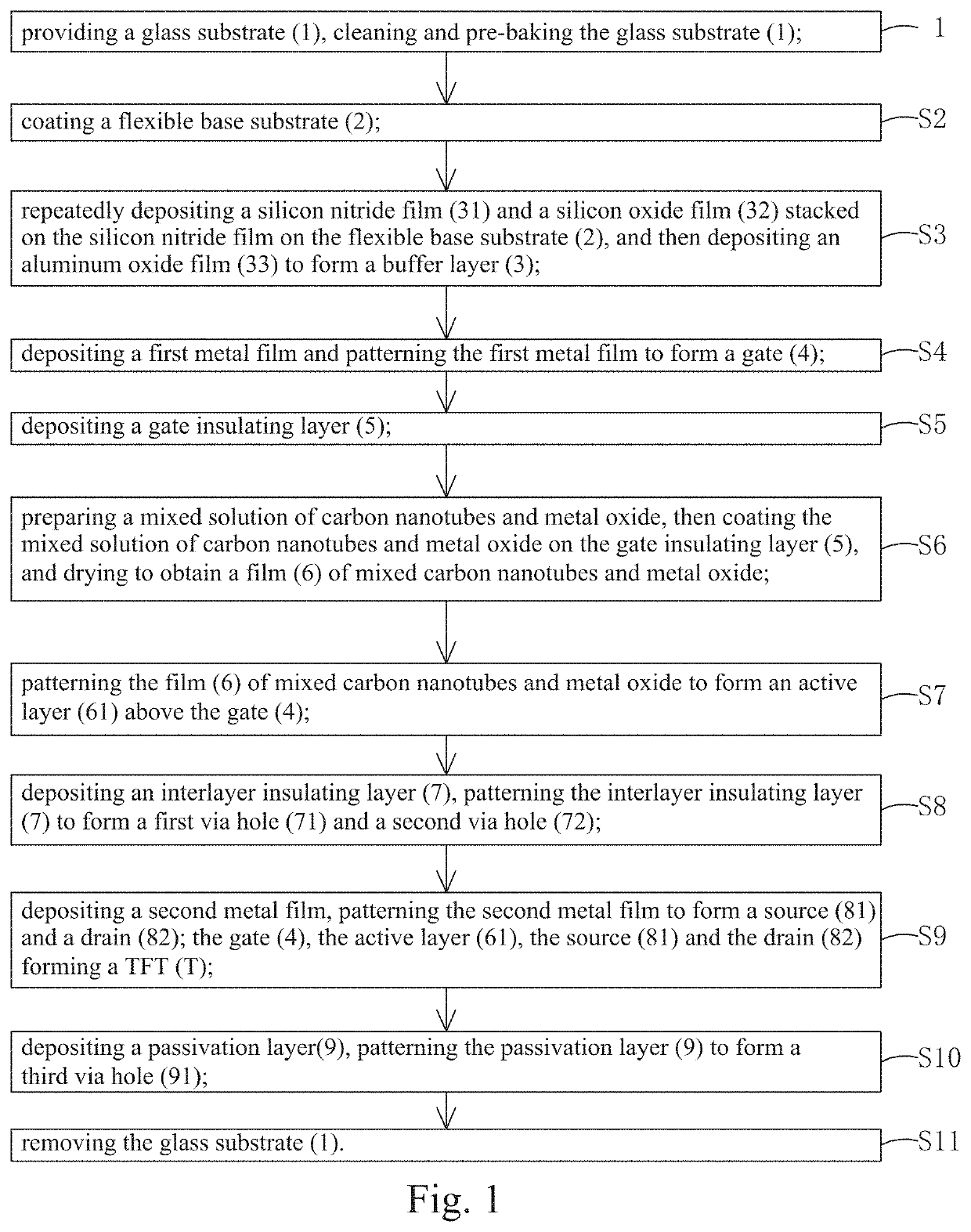
[0071]Referring to FIG. 1, the present invention provides a manufacturing method of flexible TFT backplane, comprising the steps of:

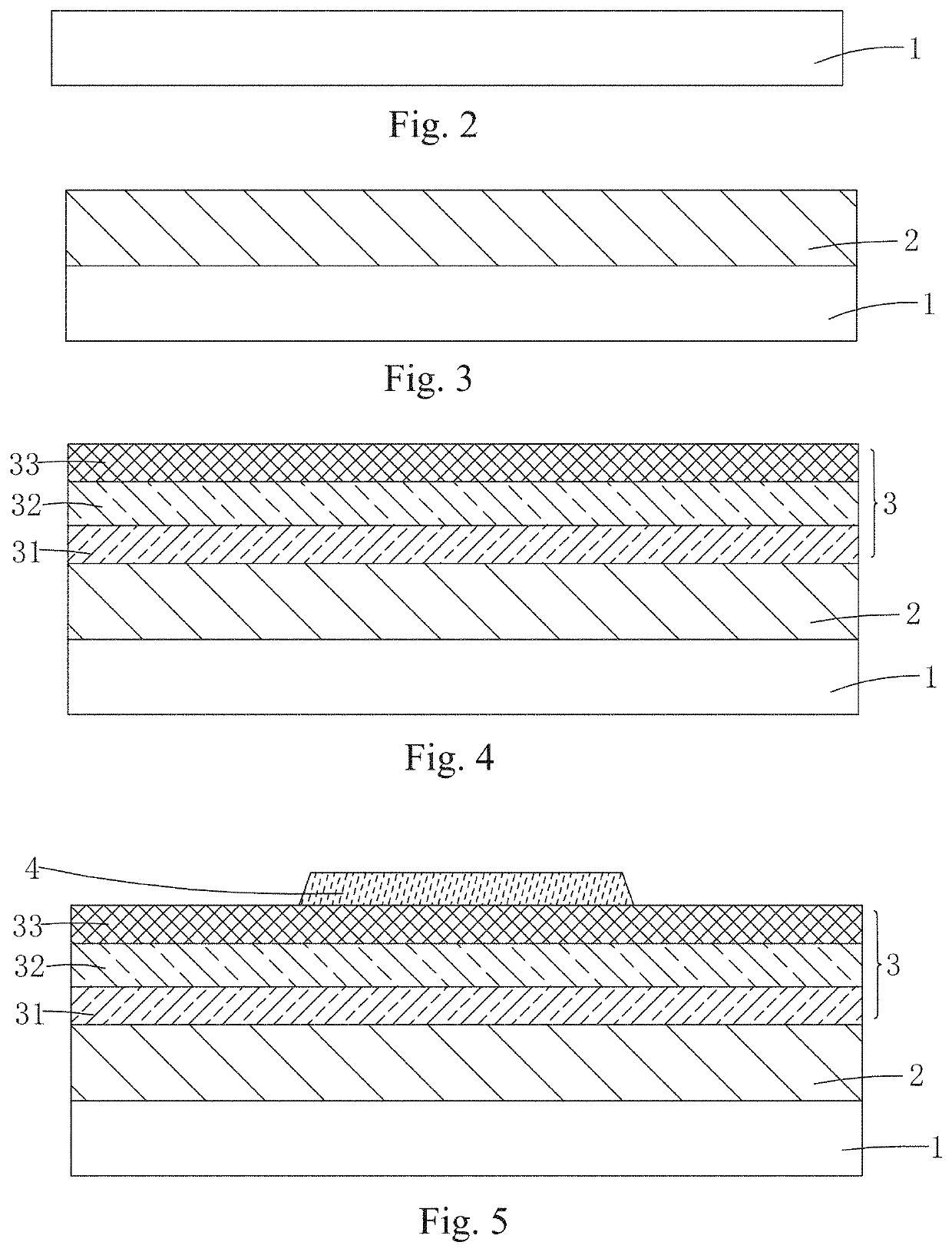
[0072]Step S1: as shown in FIG. 2, providing a glass substrate 1, cleaning and pre-baking the glass substrate 1.

[0073]Step S2: as shown in FIG. 3, coating a flexible base substrate 2 on the glass substrate 1.

[0074]Specifically, the flexible base substrate 2 is a yellow polyimide (PI) film or a transparent PI film. The yellow PI film can tolerate a higher temperature than the transparent PI film.

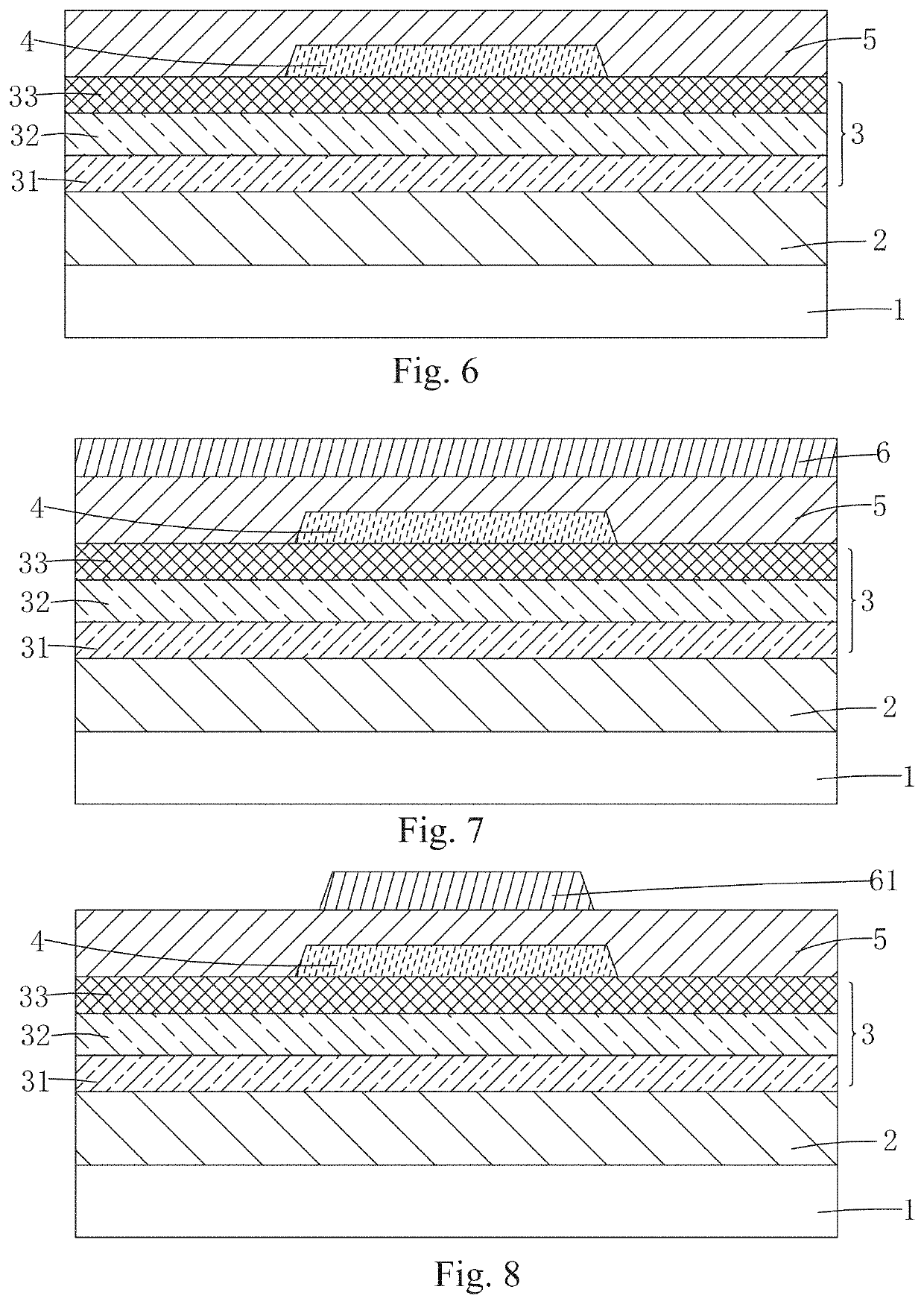
[0075]Step S3: as shown in FIG. 4, repeatedly depositing a silicon nitride film (SiNx) 31 and a silicon oxide (SiOx) film 32 stacked on the silicon nitride film 31 on the flexible base substrate 2, and then using an atomic...


PUM

PropertyMeasurementUnit
temperatureaaaaaaaaaa
flexibleaaaaaaaaaa
transparentaaaaaaaaaa

Abstract

The invention provides a manufacturing method of flexible TFT backplane. The method uses a mixed solution of carbon nanotubes and metal oxide to prepare active layer (61) of TFT (T), and the temperature is lower and will not cause damage to the flexible base substrate (2), and the material of flexible base substrate (2) is not restricted. The use of vacuum equipment is reduced to save production cost. The carbon nanotubes have excellent conductivity, and the mixture with metal oxide as the active layer (61) of the TFT can improve the electron mobility. The buffer layer (3) has a silicon nitride film (31) as the lowest layer contacting the flexible base substrate (2), making good adhesion between buffer layer (3) and flexible base substrate (2). The topmost layer of the buffer layer (3) is an aluminum oxide film (33), which enables the buffer layer (3) to resist to water.

Description

RELATED APPLICATIONS[0001]The present application is a National Phase of International Application Number PCT / CN2018 / 104485, filed Sep. 7, 2018, and claims the priority of China Application No. 201810274328.0, filed Mar. 29, 2018.BACKGROUND OF THE INVENTION1. Field of the Invention[0002]The present invention relates to the field of display techniques, and in particular to a manufacturing method of flexible thin film transistor (TFT) backplane and TFT backplane.2. The Related Arts[0003]In the field of display technology, the flat panel display technologies, such as liquid crystal display (LCD) and organic light-emitting diode (OLED), have replaced CRT displays. The OLED displays provide many advantages, such as self-luminescence, low driving voltage, high luminous efficiency, short response time, high definition and contrast ratio, a viewing angle of nearly 180°, a wide range of operating temperatures; ability to realize flexible display and large-area full-color display, and are rec...

Claims


Application Information

Patent Timeline
Patent Type & Authority Patents(United States)
IPC IPC(8): H01L29/786H01L27/32H01L51/00H01L29/66
CPCH01L29/7869H01L29/78603H01L51/0048H01L29/66969H01L27/3258H01L51/0097H01L21/77H10K59/124H10K59/12H01L29/78696H01L27/1292Y02E10/549Y02P70/50H10K59/1213H10K71/80H10K85/221H10K10/488H10K77/111
Inventor LIU, FANGMEI
Owner SHENZHEN CHINA STAR OPTOELECTRONICS SEMICON DISPLAY TECH CO LTD
Why Eureka
Try Eureka