Photocathode including field emitter array on a silicon substrate with boron layer

a photocathode and silicon substrate technology, applied in the field of low light sensing detectors, can solve the problems of low overall efficiency, inconvenient use for imaging devices such as image intensifiers, prior-art photocathodes require difficult tradeoffs between conflicting requirements, etc., to avoid significant barriers to electron escape, reduce potential barriers, and work functions well.

Active Publication Date: 2020-08-18
KLA CORP
View PDF202 Cites 11 Cited by
  • Summary
  • Abstract
  • Description
  • Claims
  • Application Information

AI Technical Summary

Benefits of technology

[0019]The present invention is directed to a photocathode structure including multiple field emitter protrusions that are integrally formed (patterned) on an output surface of a monocrystalline or polycrystalline silicon substrate, and a substantially pure boron (first) layer hermetically formed on at least tip (free end) portions of the field emitter protrusions. The introduction of integral field emitter protrusions onto the output surface circumvents the silicon substrate's relatively high work function by taking advantage of the field enhancement generated when the protrusions function as field emitters, which takes place when the substrate is subjected to an applied electric field that is high (strong) enough to reduce the potential barrier on the silicon-vacuum interface so that photoelectrons can tunnel through this barrier (quantum-mechanical tunneling) at the tip portions. The resulting emission current density can be estimated by a modified version of the Fowler-Nordheim theory, which takes into account the field enhancement factor due to the field emitters (R. Fowler and L. Nordheim, “Electron emission in intense electric fields”, Proceedings of the Royal Society of London A, Vol. 119, No. 781, May 1928, pp. 173-181). Moreover, by forming the substantially pure boron layer such that it hermetically seals at least the tip portions of the field emitter protrusions, oxidation of the field emitter output surface is substantially entirely prevented, thereby avoiding the significant barrier to electron escape encountered in conventional approaches. Thus, by producing a photocathode including field emitter protrusions integrally formed on a single-crystal silicon substrate and hermetically protected by a substantially pure boron layer, the present invention provides a photocathode having the beneficial qualities of silicon (i.e., sub-1 μm wavelength absorption, high purity / low defect material, and long electron recombination times), while avoiding the negative aspects that have previously prevented the widespread commercial use of silicon-based photocathodes.
[0020]Various conventional semiconductor processing techniques are optionally utilized to optimize the performance of photocathodes produced in accordance with the present invention. For example, the silicon substrate is preferably essentially defect-free monocrystalline (single-crystal) silicon having a thickness in the range of about 10 nm to about 100 μm, where the thickness depends in part on the wavelength of light to be captured. In a preferred embodiment, the silicon substrate includes (e.g., implanted n-type) dopants having doping levels that are optimized such that, when the photocathode is subjected to an appropriate external electric field, each field emitter protrusion functions as a field emitter in a reverse bias mode. The field emitter protrusions are formed by etching or otherwise patterning the silicon substrate such that portions of the silicon material form integral structures having relatively wide base portions integrally connected to the output surface, and extend a height distance of at least 100 nm above the output surface to relatively narrow tip (free end) portions. In one embodiment, to facilitate optimal field emitter operations, the base portion of each field emitter protrusion has a minimum diameter / width dimensions of about 100 nm and a tip portion having maximum diameter / width dimension of about 200 nm, and more preferably approximately 100 nm or less. In the exemplary embodiments, the field emitter protrusions are fabricated using standard CMOS fabrication techniques (e.g., depositing a silicon dioxide or silicon nitride mask material by PECVD on a planar substrate surface, patterning the mask using known photolithographic techniques, and then etching the silicon substrate through openings in the mask to form the field emitter protrusions) such that the field emitter protrusions are arranged in a two-dimensional array pattern on the output surface of the silicon substrate. The boron layer is preferably formed using a high temperature deposition process (e.g., between about 600° C. and 800° C.) on clean, smooth silicon in a manner that produces a pin-hole free boron layer having a thickness in the range of 1-5 nm (preferably about 2 to 3 nm), whereby the boron layer circumvents silicon's oxidation problem by reliably hermetically sealing the entire output surface of the silicon substrate against oxidation. In alternative embodiments, the field emitter protrusions are formed using various protruding structure shapes, such as rounded whiskers (cylindrical posts with round tips), rounded cones or pyramids. The various techniques and features mentioned above may be used separately or in combination to enhance photocathode performance.
[0021]According to various alternative specific embodiments of the present invention, additional layers and structures are utilized to further enhance the beneficial qualities of the inventive photocathode structure. In some embodiments, one or several gate structures (control electrodes), are disposed on the output surface and placed at, or slightly lower than, the height of the field emitter tip portions in order to achieve fast and accurate control of the emission current. In some embodiments, a second boron layer (third layer) is formed on the illuminated (first) surface of the silicon substrate to further prevent oxides and defects that can reduce photon absorption. In another embodiment, an anti-reflective material layer (fourth layer) is disposed on second boron layer (third layer) to further enhance photon absorption. In some embodiments, a metal or conductive frame or grid and a voltage source are utilized to generate an external potential difference between the illuminated surface and the output surface of the silicon substrate in order to cause electrons to preferentially move towards the output surface. In some embodiments, the photocathode includes a combination of n-type silicon field emitter and p-i-n photodiode structure that operates in an avalanche multiplication condition when a high voltage (e.g., on the order of several tens or a few hundreds of volts) is applied between the illuminated surface and the output surface of the substrate. This avalanche gain enhances the effective quantum efficient and thus improves the performance of the photocathode. In yet other embodiments, boron (or another p-type dopant) is diffused into the silicon substrate through the illuminated surface to form a p-type doped region to create a potential gradient that drives electrons away from the illuminated surface where they might recombine and be lost.
[0023]In some sensor embodiments, a second boron layer is formed on the illuminated surface of the photocathode to prevent oxide formation on the illuminated surface, and an anti-reflective material layer is provided over the second boron layer to improve photon capture efficiency. In some of these embodiments, the anti-reflective material layer is disposed between a window and the photocathode, but in other embodiments the anti-reflective material layer also serves as the sensor's receiving surface (i.e., the sensor does not have a window over the illuminated surface of the photocathode), which further increases photon capture efficiency by the sensor. In other sensor embodiments that include a window over the illuminated surface of the photocathode, an anti-reflective material layer is provided on the window to improve photon capture efficiency.
[0024]In some embodiments of the invention, a sensor including the photocathode of the present invention also includes a silicon-based detection device having an additional boron layer on its receiving surface (i.e., the surface of the detection device facing the photocathode). For example, in cases where the sensor is an electron-bombarded CCD (EBCCD) and the detection device is a CCD (which are typically formed on silicon substrates), a boron layer is formed directly on the CCD's receiving surface during fabrication to improve electron capturing efficiency of the sensor by preventing the formation of a silicon dioxide layer on the CCD's receiving surface. In other embodiments, the sensor includes a CMOS detector (i.e., instead of a CCD), and the additional boron layer is formed on the receiving surface of the CMOS detector.

Problems solved by technology

Silicon photocathodes have been made in the past, but have not found significant commercial use because, although silicon is efficient at capturing light, few of the generated electrons are able to escape from the silicon, resulting in low overall efficiency.
Although reflection photocathodes simplify some of the tradeoffs between photocathode thickness and sensitivity that are discussed below, they are not suitable for use in imaging devices such as image intensifiers and EBCCD devices (although they can be suitable for use in some photomultiplier configurations).
Prior-art photocathodes require difficult tradeoffs between conflicting requirements associated with absorbing photons and emitting photoelectrons.
A thicker photocathode increases the probability that an incident photon will be absorbed, but also increases the probability that the resulting emitted photoelectron will recombine (i.e., be lost) before it escapes.
Such a thin photocathode optimized for UV wavelengths will typically have poor sensitivity at visible and infra-red wavelengths as a significant fraction of the incident photons at longer wavelengths will pass through the photocathode without absorption.
Another limitation of prior-art photocathodes is that the energy of the emitted photoelectron varies with the wavelength of absorbed light and may be several eV when a UV photon is absorbed.
However, when an electron undergoes multiple collisions within a photocathode, it is likely to recombine and be lost due to the high level of defects within and / or on the surface of prior-art photocathode materials.
Hence, a reduced energy spread would come at the cost of substantially reduced sensitivity (most incident photons would no longer produce a signal).
One disadvantage of silicon is that silicon has a relatively large work-function (approximately 4.8 eV, Allan and Gobelli, “Work Function, Photoelectric Threshold, and Surface States of Atomically Clean Silicon”, Physical Review vol.
Silicon's relatively large band gap means that thermalized electrons cannot escape from silicon.
Even UV photons absorbed close to the surface of silicon do not create much photocurrent because the photoelectrons do not have enough energy to escape.
A second, more serious, problem with the use of silicon as a photocathode material is that silicon very readily forms a native oxide on its surface.
The interface between silicon and silicon dioxide has defects (due to dangling bonds) where the probability of an electron recombining is very high.
However, even a good quality thermal oxide has a significant defect density at its interface to silicon (typically 109 to 1011 defects per cm2), and the high band gap of the oxide combined with a minimum thickness of close to 2 nm still provides a significant barrier to electrons escaping even if the work-function can be overcome.
For these reasons, silicon has never found significant commercial use as a photocathode.

Method used


Image

  • Photocathode including field emitter array on a silicon substrate with boron layer
  • Photocathode including field emitter array on a silicon substrate with boron layer
  • Photocathode including field emitter array on a silicon substrate with boron layer

Examples


Embodiment Construction

[0039]The present invention relates to an improvement in low light sensors for semiconductor inspection systems. The following description is presented to enable one of ordinary skill in the art to make and use the invention as provided in the context of a particular application and its requirements. As used herein, directional terms such as “top”, “bottom”, “over”, “under”, “upper”, “upward”, “lower”, “down” and “downward” are intended to provide relative positions for purposes of description, and are not intended to designate an absolute frame of reference. Various modifications to the preferred embodiment will be apparent to those with skill in the art, and the general principles defined herein may be applied to other embodiments. Therefore, the present invention is not intended to be limited to the particular embodiments shown and described, but is to be accorded the widest scope consistent with the principles and novel features herein disclosed.

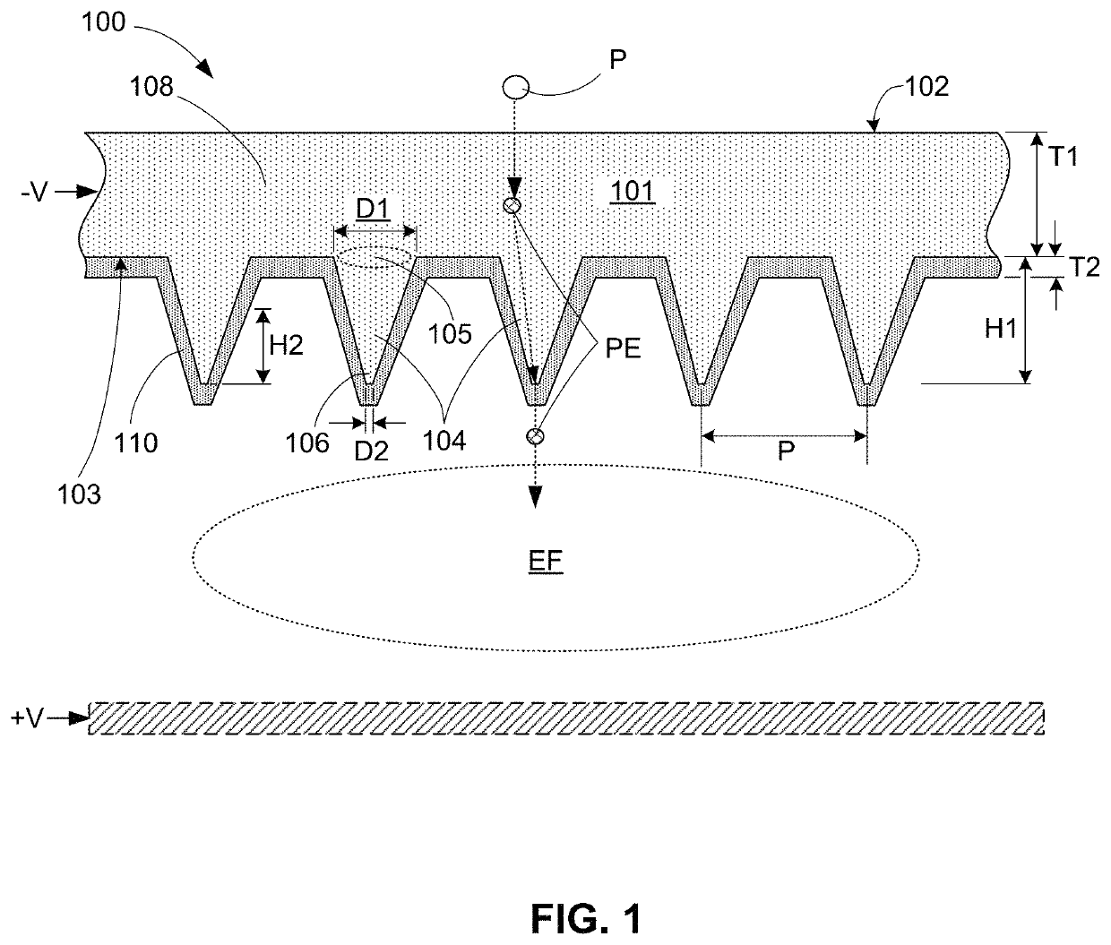
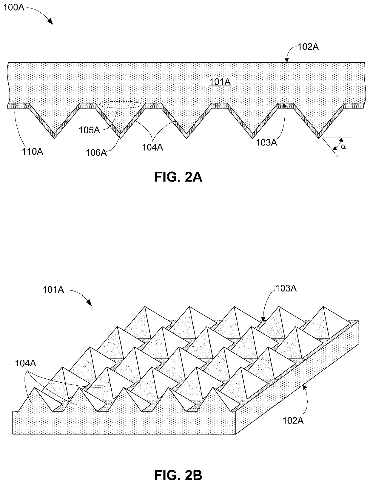
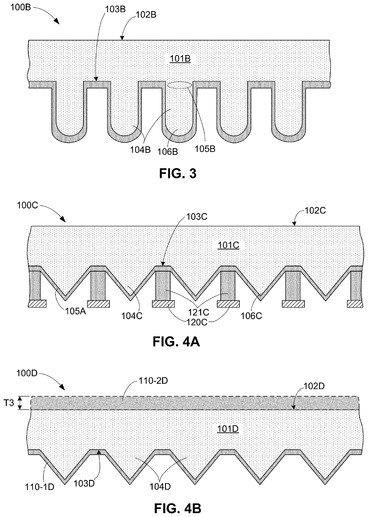
[0040]FIG. 1 illustrates, in cros...


PUM

PropertyMeasurementUnit
thicknessaaaaaaaaaa
energyaaaaaaaaaa
wavelengthsaaaaaaaaaa

Abstract

A photocathode utilizes an field emitter array (FEA) integrally formed on a silicon substrate to enhance photoelectron emissions, and a thin boron layer disposed directly on the output surface of the FEA to prevent oxidation. The field emitters are formed by protrusions having various shapes (e.g., pyramids or rounded whiskers) disposed in a two-dimensional periodic pattern, and may be configured to operate in a reverse bias mode. An optional gate layer is provided to control emission currents. An optional second boron layer is formed on the illuminated (top) surface, and an optional anti-reflective material layer is formed on the second boron layer. An optional external potential is generated between the opposing illuminated and output surfaces. An optional combination of n-type silicon field emitter and p-i-n photodiode film is formed by a special doping scheme and by applying an external potential. The photocathode forms part of sensor and inspection systems.

Description

PRIORITY APPLICATION[0001]This application claims priority to U.S. Provisional Patent Application 62 / 164,975, filed May 21, 2015, entitled “PHOTOCATHODE INCLUDING FIELD EMITTER ARRAY ON A SILICON SUBSTRATE WITH BORON LAYER”, and incorporated by reference herein.RELATED APPLICATIONS[0002]This application is related to U.S. patent application Ser. No. 14 / 198,175 (published as 2014 / 0291493), entitled “Photomultiplier Tube, Image Sensor, and an Inspection System Using a PMT or Image Sensor”, and filed by Chuang et al. on Mar. 5, 2014, and to U.S. patent application Ser. No. 13 / 947,975 (published as 2014 / 0034816), entitled “Photocathode Including Silicon Substrate with Boron Layer” and filed by Chuang et al. on Jul. 22, 2013. Both of these applications are included by reference herein.BACKGROUND OF THE INVENTIONField of the Invention[0003]The present invention generally relates to low light sensing detectors (sensors) used in conjunction with semiconductor wafer, reticle or photomask ins...

Claims


Application Information

Patent Timeline
Patent Type & Authority Patents(United States)
IPC IPC(8): H01J1/308H01L31/107H01L31/105H01L27/148H01J1/34H01J1/304
CPCH01L31/105H01J1/308H01L27/14831H01L31/107H01J1/3044H01J1/34H01J2201/3423H01J31/50H01J29/385H01J31/26G02B21/125H01L27/14643H01L27/148
Inventor CHUANG, YUNG-HO ALEXFIELDEN, JOHNXIAO-LI, YINYINGLIU, XUEFENG
Owner KLA CORP
Why Eureka
Try Eureka