Method for hybrid wafer-to-wafer bonding

a bonding method and wafer technology, applied in the direction of basic electric elements, electrical equipment, semiconductor devices, etc., can solve the problems of high risk, high investment and high risk of cutting-edge technologies, and exclude many small and medium-sized integrated circuit manufacturers, and achieve sufficient metal bonding, shorten the annealing process time of bonding metal, and reduce the risk of dielectric delamination caused by thermal expansion mismatch

Active Publication Date: 2020-10-06
SHANGHAI INTEGRATED CIRCUIT RES & DEV CENT
View PDF6 Cites 4 Cited by
  • Summary
  • Abstract
  • Description
  • Claims
  • Application Information

AI Technical Summary

Benefits of technology

[0008]To overcome the defects in the prior art, a hybrid bonding method between silicon wafers is provided to reduce the risk of dielectric stratification by reducing the annealing temperature of the metal, thereby reducing the difficulty of the process integration.
[0025]According to the method for the hybrid wafer-to-wafer bonding of the present invention, a part of the Cu on the surface of the Cu pattern structure is removed by adopting an etching process, the bonding metal is selectively deposited, and the lower crystallization temperature and the shorter annealing process time of the bonding metal are utilized, so as to that the sufficient metal bonding can be obtained at low annealing temperature, and the dielectric delaminating risk caused by thermal expansion mismatch is further reduced, the difficulty of the process integration is reduced, the process time is saved, and the product yield is improved.

Problems solved by technology

The high investment and high risk of these cutting-edge technologies have excluded many small and medium-sized integrated circuit manufacturers.
Although the yield of the chip-to-chip bonding is high, the dicing and testing need to take a lot of time and resources, so the manufacturing cost is very high.
But if the yield of the silicon wafers is not high or unstable, the number of KGD (known good die) will be limited, which will affect the qualified rate of wafer-to-wafer bonding.
However, the final annealing process takes too long, which seriously affects the production efficiency.
In addition, since the thermal expansion coefficient of the Cu is much higher than that of the SiO2 dielectric, at the annealing temperature of the Cu crystallization, the volume of the Cu will increase and may push out the already bonded dielectric around, resulting in defects and even the failure of the bonding process.
The above hybrid bonding technology has very marginal process control requirements for the Cu CMP process, the height of the Cu layer is required to be lower than that of the dielectric layer, and the recessed amount of the Cu is within 10 nm, which brings severe challenges to the process control in mass production.

Method used


Image

  • Method for hybrid wafer-to-wafer bonding
  • Method for hybrid wafer-to-wafer bonding
  • Method for hybrid wafer-to-wafer bonding

Examples


Embodiment Construction

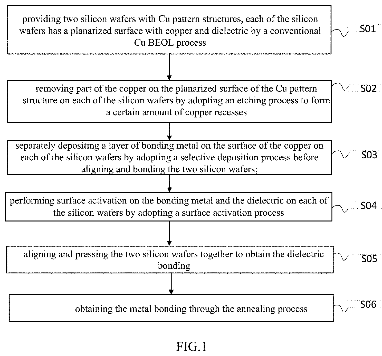
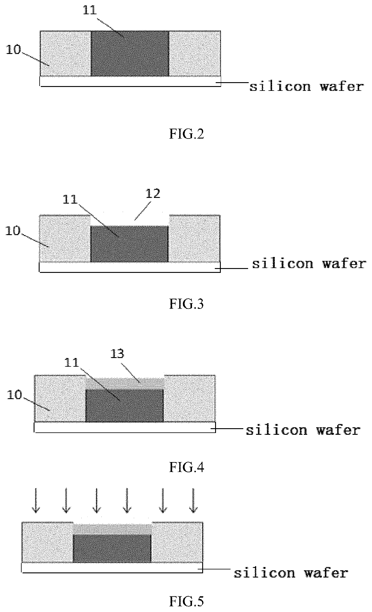
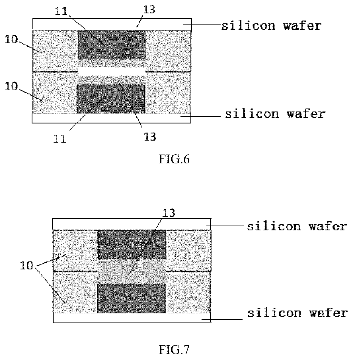
[0028]The contents of the present invention will be described in further detail below with reference to the accompanying drawings. The present invention can have various changes in different examples, is not separated from the scope of the invention, and the description and illustration thereof are intended to be illustrative in nature and not to limit the invention. It should be noted that the drawings both adopt a very simplified form and use a non-precise ratio, to facilitate the purpose of describing the embodiments of the present invention in a convenient and clear manner.

[0029]In the following detailed description of the present invention, please refer to FIG. 1, FIG. 1 is a flow chart of a method for hybrid wafer-wafer bonding according to the present invention. At the same time, please refer to FIGS. 2-7, FIGS. 2-7 are schematic views of a process for performing the hybrid bonding between two silicon wafers according to the method shown in FIG. 1. As shown in FIG. 1, the met...


PUM

PropertyMeasurementUnit
temperatureaaaaaaaaaa
heightaaaaaaaaaa

Abstract

A method for hybrid wafer-to-wafer bonding, comprising: providing two silicon wafers with Cu pattern structures, a conventional Cu BEOL process is adopted on the silicon wafers to obtain the planarized surface with copper and dielectric; removing part of the Cu on the planarized surface of the Cu pattern structures by adopting an etching process to form a certain amount of Cu recesses; depositing a layer of bonding metal on the surface of the Cu by adopting a selective deposition process; performing surface activation on the bonding metal and the dielectric by adopting a surface activation process; aligning and pressing the two silicon wafers together to obtain the dielectric bonding; and obtaining the metal bonding through the annealing process. The sufficient metal bonding can be obtained at low annealing temperature according to the present invent, thereby the risk of dielectric delaminating caused by thermal expansion mismatch is reduced, which is conducive to reduce the difficulty of process integration, save process time and improve product yield.

Description

CROSS-REFERENCE TO RELATED APPLICATION[0001]This application claims the priority benefit of International Patent Application Serial No. PCT / CN2017 / 087280, filed Jun. 6, 2017, which is related to and claims the priority benefit of China patent application serial No. 201610948181.X, filed Oct. 26, 2016. The entirety of each of the above-mentioned patent applications is hereby incorporated by reference herein and made a part of this specification.FIELD OF THE INVENTION[0002]The invention relates to the field of integrated circuit manufacturing technology, and more specifically, relates to a wafer-wafer bonding method adopting a hybrid bonding mode.BACKGROUND OF THE INVENTION[0003]With the integrated circuit manufacturing technology entering into 45 nm and the following generation, in order to overcome technical problems caused by feature size reduction, the industry has generally adopted some new technologies, such as a strain silicon engineering, a high dielectric constant dielectric / ...

Claims


Application Information

Patent Timeline
Patent Type & Authority Patents(United States)
IPC IPC(8): H01L21/00H01L21/18H01L21/768H01L21/324
CPCH01L21/185H01L21/324H01L21/76876H01L21/76895H01L2224/80895H01L2224/83896H01L2224/32145H01L2224/08145H01L24/08H01L24/80H01L24/83H01L24/94H01L24/05H01L2224/05647H01L24/03H01L2224/8034H01L2224/80986H01L2224/05541H01L21/2007
Inventor LIN, HONG
Owner SHANGHAI INTEGRATED CIRCUIT RES & DEV CENT
Why Eureka
Try Eureka