
Organic electroluminescent device, thin luminous film, display apparatus, and lighting apparatus

a technology of electroluminescent devices and light sources, which is applied in the direction of organic semiconductor devices, organic chemistry, group 5/15 element organic compounds, etc., can solve the problems of compound, unsatisfactory blue light-emitting efficiency or molecular stability, and the inability to use tadf mechanisms in organic el devices. , to achieve the effect of high emission efficiency, low cost and low cos

Active Publication Date: 2020-12-08
MERCK PATENT GMBH
View PDF34 Cites 1 Cited by
  • Summary
  • Abstract
  • Description
  • Claims
  • Application Information

AI Technical Summary

Benefits of technology

The present invention provides an organic electroluminescent device with high efficiency and stability. This invention also provides a thin luminous film containing a π-conjugated compound for use in the organic electroluminescent device. Additionally, this invention provides display and lighting apparatuses that include the organic electroluminescent device. The π-conjugated compound described in this invention has a unique structure that allows for efficient electron transition between the HOMO and the LUMO, resulting in high emission efficiency.

Problems solved by technology

Unfortunately, the achievement of high quantum efficiency in a phosphorescent mode requires the use of a complex of a rare metal (e.g., iridium or platinum) as a central metal, which may cause future problems in the industry in terms of the reserves and prices of rare metals.
Unfortunately, the TADF mechanism has not yet been practically used in organic EL devices because of problems derived from luminous materials exhibiting TADF and problems upon application of the mechanism to organic EL devices.
Such a compound, however, is still unsatisfactory in terms of blue light-emitting efficiency or molecular stability.
In general, difficulty is encountered in injecting holes into a luminous material contained in a luminous layer if the HOMO level of the luminous material is lower than that of a hole transporting layer.
In any case, difficulty is encountered in injecting holes into the luminous layer.
Even if emission quantum efficiency is improved, high driving voltage leads to difficulty in increasing power efficiency [lm / W], resulting in failure to reduce power consumption.
The delayed fluorescence mechanism encounters problems including technical difficulty in the design of a luminous material and a few alternatives of the host compound used in combination with the luminous material.
The technical development of a blue light-emitting material is the most difficult hurdle.
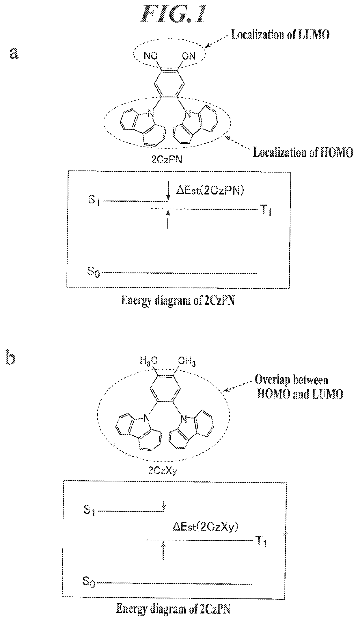
The complete separation of the HOMO and the LUMO, however, leads to reduced electron transition between the HOMO and the LUMO (i.e., generation of few excitons), resulting in insufficient emission intensity despite the occurrence of TADF.
Although both the occurrence of TADF and high emission intensity are achieved in a traditional compound by the molecular design for appropriate overlap between the HOMO and the LUMO, difficulty is encountered in the design of a TADF molecule exhibiting practical emission intensity and efficiency; i.e., the molecular design has room for improvement.

Method used


Image

  • Organic electroluminescent device, thin luminous film, display apparatus, and lighting apparatus
  • Organic electroluminescent device, thin luminous film, display apparatus, and lighting apparatus
  • Organic electroluminescent device, thin luminous film, display apparatus, and lighting apparatus

Examples


example 1

(Preparation of Organic EL Device 1-1)

[0527]An indium tin oxide (ITO) anode having a thickness of 150 nm was formed on a glass substrate (50 mm by 50 mm, thickness: 0.7 mm), followed by patterning. The transparent substrate provided with the transparent ITO electrode was ultrasonically cleaned in isopropyl alcohol, dried with dry nitrogen gas, and then subjected to UV ozone cleaning for five minutes. The resultant transparent substrate was fixed to a substrate holder of a commercially available vacuum vapor deposition apparatus.

[0528]Materials for layers were placed in vapor deposition crucibles in the vacuum vapor deposition apparatus in amounts suitable for preparation of an organic EL device. The crucibles were composed of molybdenum or tungsten; i.e., a material for resistance heating.

[0529]The apparatus was evacuated to a vacuum of 1×10⁻⁴ Pa, and a vapor deposition crucible containing α-NPD was heated by energization. α-NPD was vapor-deposited onto the ITO transparent electrode...

example 2

[0553](Preparation of Organic EL Device 2-1)

[0554]An indium tin oxide (ITO) anode having a thickness of 150 nm was formed on a glass substrate (50 mm by 50 mm, thickness: 0.7 mm), followed by patterning. The transparent substrate provided with the transparent ITO electrode was ultrasonically cleaned in isopropyl alcohol, dried with dry nitrogen gas, and then subjected to UV ozone cleaning for five minutes. The resultant transparent substrate was fixed to a substrate holder of a commercially available vacuum vapor deposition apparatus.

[0555]Materials for layers were placed in vapor deposition crucibles in the vacuum vapor deposition apparatus in amounts suitable for preparation of an organic EL device. The crucibles were composed of molybdenum or tungsten; i.e., a material for resistance heating.

[0556]The apparatus was evacuated to a vacuum of 1×10⁻⁴ Pa, and a vapor deposition crucible containing α-NPD was heated by energization. α-NPD was vapor-deposited onto the ITO transparent ele...

example 3

[0574]Red light-emitting organic EL device 2-10, green light-emitting organic EL device 2-4, and blue light-emitting organic EL device 2-7, which were prepared in Example 2, were arranged on a single substrate, to prepare an active matrix full-color display apparatus illustrated in FIG. 8. FIG. 8 is a schematic illustration of display A of the full-color display apparatus. In detail, the display has, on a single substrate, a wiring unit including a plurality of scanning lines 5 and data lines 6, and a plurality of arranged pixels 3 (red light-emitting, green light-emitting, and blue light-emitting pixels). The scanning lines 5 and data lines 6 of the wiring unit are composed of a conductive material and are orthogonal to each other to form a grid pattern. The scanning lines 5 and the data lines 6 are connected to the pixels 3 at orthogonal intersections (details are not illustrated). The pixels 3 are driven by the active matrix system including the organic EL devices that emit light...


PUM


Abstract

An organic electroluminescent device contains an anode, a cathode, and an organic layer containing at least one luminous layer. The organic layer is disposed between the anode and the cathode. At least one luminous layer contains a π-conjugated compound exhibiting no overlap between the electron density distributions of the HOMO and the LUMO in the molecule, such that electron transition between the HOMO and the LUMO occurs by a through-space interaction in the molecule. The π-conjugated compound has a π-conjugated aromatic ring at a moiety on which at least one of the HOMO and the LUMO is localized.

Description

CROSS REFERENCE TO RELATED APPLICATION[0001]This Application is a 371 of PCT / JP2015 / 071647 filed on Jul. 30, 2015, which, in turn, claimed the priority of Japanese Patent Application No. JP 2014-156059 filed on Jul. 31, 2014, both applications are incorporated herein by reference.TECHNICAL FIELD[0002]The present invention relates to an organic electroluminescent device, a thin luminous film, a display apparatus, and a lighting apparatus, each of the apparatuses including the organic electroluminescent device. In particular, the present invention relates to an organic electroluminescent device exhibiting improved emission efficiency and high stability, a thin luminous film, a display apparatus, and a lighting apparatus, each of the apparatuses including the organic electroluminescent device.BACKGROUND ART[0003]Organic electroluminescent (hereinafter may be referred to as “EL”) devices, which are based on electroluminescence of organic materials, have already been put into practice as...

Claims


Application Information

Patent Timeline
Patent Type & Authority Patents(United States)
IPC IPC(8): H01L51/00C07F9/6568C07F7/08C07D491/22C07D471/14C07D471/04C07D413/14C07D409/14C07D405/10C07D403/10C07D401/10C07D333/76C07D311/90C07D219/02C07D403/14C07D413/10C07D209/86C07D403/12H05B33/20H05B33/14C09K11/06C07D487/04H01L51/50H10K99/00
CPCC07D471/14C07D311/90H01L51/0094C07D413/14H01L51/0072C09K11/06C07D403/14H01L51/0068C07D333/76H01L51/0069C07D471/04H05B33/14H01L51/0071C07D413/10H01L51/0074H01L51/0061C07D487/04H05B33/20C07D403/10C07F7/0812C07F9/65685C07D219/02C07D491/22C07D209/86H01L51/0067H01L51/0073C07D405/10C07D401/10C07D409/14C07D403/12H01L51/0052H01L51/5016H01L2251/552C09K2211/1029H01L51/5012H01L51/5028H10K85/615H10K85/654H10K85/6574H10K85/6572H10K85/40H10K50/11H10K2101/30C07D498/22C09K2211/1044H10K50/00H10K85/636H10K85/655H10K85/656H10K85/657H10K85/6576H10K50/121H10K2101/10
Inventor OSHIYAMA, TOMOHIROKITA, HIROSHINAMIKAWA, TAKETOOKUYAMA, MICHIHIROHATTORI, TATSUYAMIYATA, YASUO
Owner MERCK PATENT GMBH
Learn More