Electron gun and electron microscope

a technology of electron microscope and electron gun, which is applied in the direction of electrical equipment, electric discharge tubes, basic electric elements, etc., can solve the problems of inefficient power consumption, wide energy spread, and high speed inspections performed during ic production typically take one hour or less, and achieves a wide range of electrons. , the effect of reducing the band gap

Active Publication Date: 2021-03-09
KLA CORP +1
View PDF223 Cites 1 Cited by
  • Summary
  • Abstract
  • Description
  • Claims
  • Application Information

AI Technical Summary

Benefits of technology

[0015]The present invention is directed to an electron gun for use in SEMs or other devices / instruments, where the electron gun includes a field emitter (cathode) having one or more field emitter protrusions integrally connected to a monocrystalline (single crystal) silicon substrate such that the protrusion(s) extending from an output (second) surface of the silicon substrate, and a substantially pure silicon-carbide (SiC) layer (i.e., consisting of at least 75% SiC) hermetically disposed on at least a tip (free end) portion of the field emitter protrusion. The SiC layer is formed on the protrusion(s) such that, during operation, electrons leaving the monocrystalline silicon substrate through the tip portion only pass through the SiC layer before forming a primary electron beam. The integral connection of the field emitter protrusion to the silicon substrate (i.e., by way of etching portions of the single crystal silicon substrate such that a remaining un-etched portion of single crystal silicon forms the protrusion) circumvents the silicon substrate's relatively high work function by taking advantage of the field enhancement generated when the substrate is subjected to an applied external electric field that is high (strong) enough to reduce the potential barrier outside the tip portion, whereby electrons are able to tunnel through the reduced potential barrier (i.e., by way of quantum-mechanical tunneling). Moreover, the use of a contiguous substantially pure SiC layer to hermetically seal the field emitter protrusion provides several advantages over conventional surface treatments and coatings: first, various techniques are known for forming a substantially pure SiC layer as a pin-hole free coating that prevents the formation of native oxide on the output surface of the field emitter protrusion; second, substantially pure SiC layer has a lower bandgap than conventional coatings such as silicon dioxide, thereby increasing the flow of electrons during operation; and third, the SiC layer can withstand processing temperatures over 400° without significant change in its composition or work-function allowing for vacuum bakeout of an electron gun incorporating such an emitter at temperatures of 200° C. or higher. Thus, by producing an electron gun with a field emitter including field emitter protrusions integrally formed on a single-crystal silicon substrate and hermetically protected by a substantially pure SiC layer, the present invention facilitates the production of cold electron guns having the beneficial qualities of silicon (i.e., sub-1 μm wavelength absorption, high purity / low defect material, and long electron recombination times), while avoiding the negative aspects that have previously prevented the widespread commercial production of cold electron guns that utilize coated silicon field emitters.
[0016]The electron gun of the present invention circumvents silicon's relatively high work function by taking advantage of the field enhancement due to the field emitter protrusion. A second electrode (i.e., the anode) is positioned facing the field emitter cathode. The anode may be made of a metal such as tungsten, molybdenum, or stainless steel. A high voltage source, typically on the order of kilovolts, is utilized to generate an external potential difference between the field emitter protrusion and the anode in order to create a strong electric field near the tip of the field emitter protrusion causing electrons to preferentially move toward the emitter tip. When a high potential difference between the field emitter protrusion and anode (such as a voltage of about 1 kV or higher) is used, the anode should preferably be about 50 μm away from the field emitter protrusion. In one embodiment, the anode is placed at least 50 μm from the emitter tip, at a positive voltage of at least 500 V relative to the field emitter protrusion. In an alternative embodiment, the anode is placed close to the emitter tip, such as a distance of about 2 μm or less, at a potential of less than 100 V positive to the emitter. Placing the anode closer to the emitter tip allows a sufficiently strong electric field to be generated from a smaller voltage, which has the advantage of minimizing back-bombardment of the emitter by highly energetic ions that can reduce the lifetime of the emitter. However, placing the anode closer to the emitter tip requires more precise alignment of the aperture in the anode relative to the emitter tip.
[0017]Field emission takes place when the applied electric field is high enough to reduce the potential barrier on the silicon-vacuum interface so that the electron can tunnel through this barrier (i.e., quantum-mechanical tunneling). In a semiconductor, where the electron concentration is determined by the local doping level and potential, it is possible to configure field emitters to be operated in reverse bias mode as in a p-n diode, in which a depletion layer is generated due to the high electric field at the emitter surface. The interface between vacuum and a SiC-coated, p-type doped field emitter protrusion can form a p-n junction, in which the vacuum is considered to be an n-type medium. In this case, the conduction and valence bands will bend downward at the surface. If the electric field is sufficient to bring the bottom of the conduction band below the Fermi energy level, there will be an abundance of electrons at the apex of the emitter tip, and an electric current, on the order of nA to μA is produced. In an alternative embodiment, the electric field may be kept at a slightly lower level so that the bottom of the conduction band stays just above the Fermi level and little or no emission current is generated. In this embodiment, light may be used to create electron-hole pairs. The electrons so created will be strongly attracted towards the tip and many will be emitted from the tip as an emission current. In this embodiment, the emission current may be controlled by controlling the light level incident on, or near, the field emitter substrate. In yet another embodiment, the bulk of the silicon wafer may be n-type doped, so that an abundance of electrons is available to form the emission current. The emission current density can be estimated by a modified version of the Fowler-Nordheim theory, which takes into account the field enhancement factor due to the field emitter protrusion. Thus, by producing an electron emitter structure having both a SiC layer and a field emitter protrusion formed on the single-crystal silicon substrate, the present disclosure provides the beneficial qualities of silicon (i.e., high purity / low defect material, long electron recombination times, and mature silicon-based fabrication process), and enables the enticing features of field emitters (i.e., small emitter size, low power consumption, high brightness, high current density, high speed, and long emitter lifetime), while avoiding the negative aspects that have previously prevented the widespread commercial use of silicon-based field emitter structures.
[0018]According to various alternative embodiments of the present disclosure, various additional layers and structures are utilized to further enhance the beneficial qualities of the disclosed emitter structure. In some embodiments, one or several gate layers, or control electrodes, are placed at, slightly lower than, or slightly lower than the height of the field emitter protrusion (i.e., from base to tip) in order to further enhance the electric field at the emitter tip, and to achieve fast and accurate control of the emission current. The gate layer is typically formed on top of one or several insulating layers deposited on the substrate. If there are several gate layers, the insulating layers are the spacers in between these gate layers. In yet other embodiments, multi electron-beam guns comprise a plurality of the disclosed field emitter protrusions arranged in a two-dimensional periodic pattern (e.g., a Field Emitter Array (FEA)) disposed on the emitter surface for emitting electrons in the presence of an electric field.

Problems solved by technology

For example, high speed inspections performed during IC production typically take one hour or less.
Thermionic emitters typically require elevated temperatures (greater than 1300° K) to operate, and have several drawbacks such as inefficient power consumption, wide energy spread, short lifetime, low current density, and limited brightness.
Nevertheless, metallic emitters suffer from several disadvantages such as lack of uniformity due to metal deposition techniques, and, more severely, degradation in emission current, mainly due to oxidation.
Even though silicon field emitters have shown promise in recent years, they are not yet commercially available.
One serious problem with the use of silicon to form field emitters is that silicon is quite reactive, and can be contaminated within hours, even at pressures around 10−10 torr (see for instance, J. Shaw, and J. Itoh, “Silicon Field Emitter Arrays,” in Vacuum Microelectronics, W. Zhu, ed.
The interface between silicon and silicon dioxide has defects (due to dangling bonds) where the probability of an electron recombination is very high.
These aforementioned problems may result in low brightness and current as well as poor stability, reliability, scalability and uniformity, and have hindered the commercial use of silicon field emitters.
This presents a particularly significant problem in the semiconductor industry, where inspection / review / lithography instruments are expected to operate continuously and stably without interruption for long periods.
However, these coating materials are usually limited by the fabrication process in forming smooth and uniform coating surfaces, and / or are often affected by the oxide layer formed on the coating surfaces, creating an additional energy barrier.
For these reasons, cold electron guns that utilize coated silicon field emitters have not yet become practical.

Method used


Image

  • Electron gun and electron microscope
  • Electron gun and electron microscope
  • Electron gun and electron microscope

Examples


Embodiment Construction

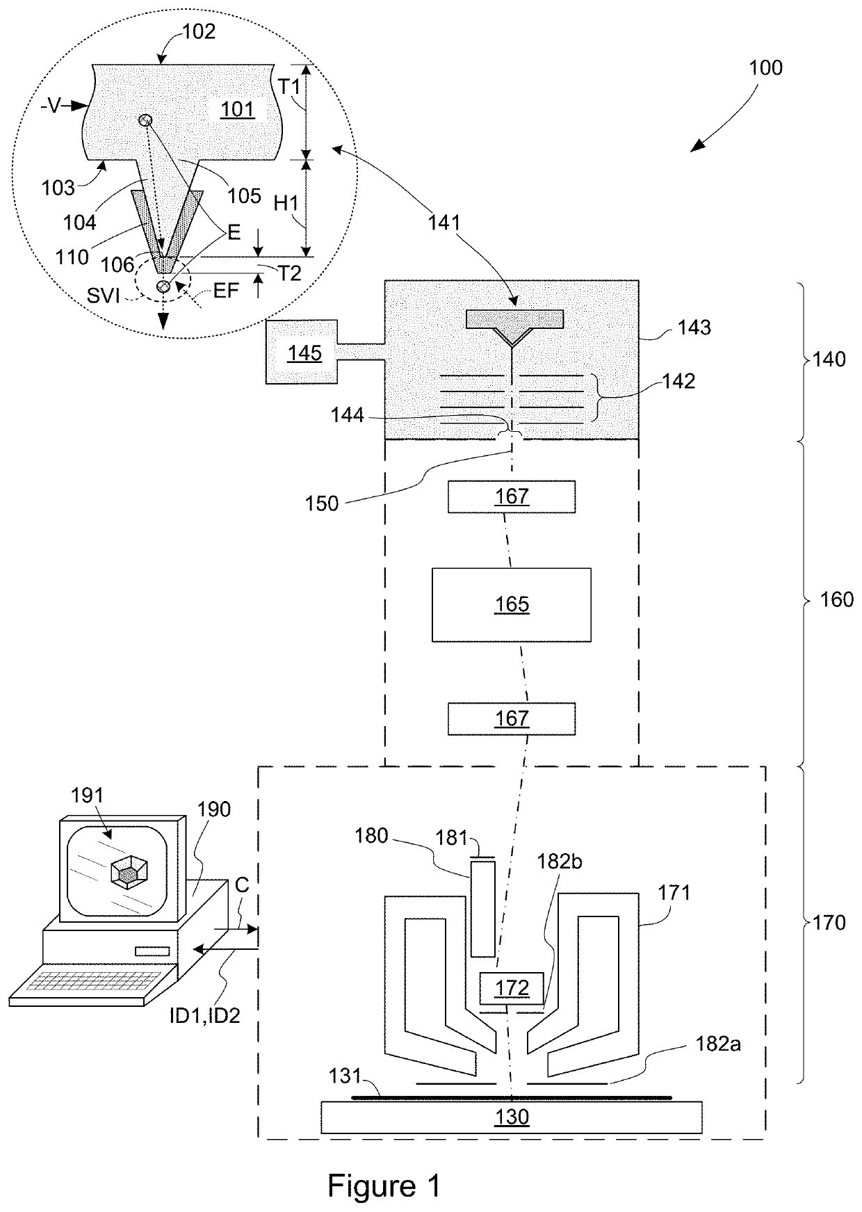
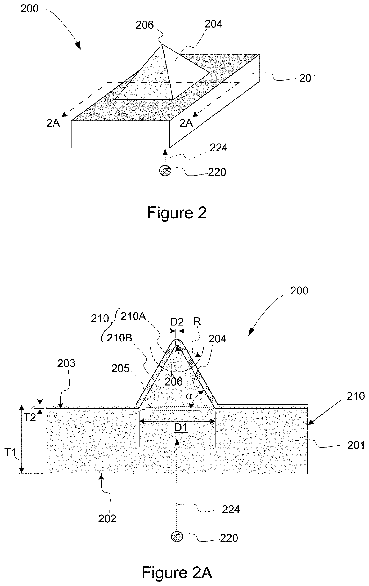
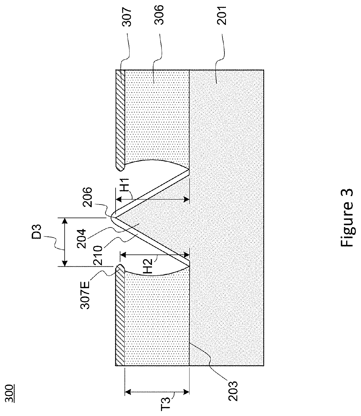
[0028]Although claimed subject matter will be described in terms of certain embodiments, other embodiments, including embodiments that do not provide all of the benefits and features set forth herein, are also within the scope of this disclosure. Various structural, logical, process step, and electronic changes may be made without departing from the scope of the disclosure. Accordingly, the scope of the disclosure is defined only by reference to the appended claims.

[0029]The following description is presented to enable one of ordinary skill in the art to make and use the disclosure as provided in the context of a particular application and its requirements. As used herein, directional terms such as “top,”“bottom,”“over,”“under,”“upper,”“upward,”“lower,”“down,” and “downward” are intended to provide relative positions for purposes of description, and are not intended to designate an absolute frame of reference. Various modifications to the preferred embodiment will be apparent to tho...


PUM


Abstract

An electron gun for an electron microscope or similar device includes a field emitter cathode having a field emitter protrusion extending from the output surface of a monocrystalline silicon substrate, and electrodes configured to enhance the emission of electrons from a tip portion of the field emitter protrusion to generate a primary electron beam. A thin, contiguous SiC layer is disposed directly on at least the tip portion of the field emitter protrusion using a process that minimizes oxidation and defects in the SiC layer. Optional gate layers may be placed at, slightly lower than or slightly higher than the height of the field emitter tip portion to achieve high emission current and fast and accurate control of the primary emission beam. The field emitter can be p-type doped and configured to operate in a reverse bias mode, or the field emitter can be n-type doped.

Description

RELATED APPLICATION[0001]This application claims priority from U.S. Provisional Patent Application No. 62 / 744,890, entitled “ELECTRON SOURCE”, which was filed on Oct. 12, 2018, and is incorporated by reference herein. This application also claims priority from U.S. Provisional Patent Application No. 62 / 885,624, entitled “ELECTRON GUN AND ELECTRON MICROSCOPE”, which was filed on Aug. 12, 2019, and is incorporated by reference herein.FIELD OF THE DISCLOSURE[0002]The disclosure relates generally to electron guns suitable for use in scanning electron microscopes, electron-beam lithography systems, and other systems suitable for reviewing and inspecting samples (e.g., photomasks, reticles, and semiconductor wafers). In particular, the disclosure relates to electrons guns that utilize cold electron field emitters, and to review and inspection systems including these electron guns.BACKGROUND OF THE DISCLOSURE[0003]The integrated circuit industry requires inspection tools with increasingly ...

Claims


Application Information

Patent Timeline
Patent Type & Authority Patents(United States)
IPC IPC(8): H01J37/073H01J37/28H01J37/317
CPCH01J37/073H01J37/28H01J37/3174H01J2237/06341H01J2237/0635
Inventor CHUANG, YUNG-HO ALEXXIAO-LI, YINYINGGARCIA BERRIOS, EDGARDOFIELDEN, JOHNNAGAO, MASAYOSHI
Owner KLA CORP
Why Eureka
Try Eureka