Photomask blank, manufacturing method of photomask and photomask

a manufacturing method and technology of photomasks, applied in the field of photomask blanks, photomask manufacturing methods, etc., can solve the problems of fine pattern collapse, deterioration of photomask resolution, and worsening of resolution limits

Active Publication Date: 2022-08-02
SHIN ETSU CHEM IND CO LTD
View PDF14 Cites 0 Cited by
  • Summary
  • Abstract
  • Description
  • Claims
  • Application Information

AI Technical Summary

Benefits of technology

[0011]The cause of deteriorating the resolution of the photomask comes from a problem caused by the chrome film in addition to the above. In the dry etching process of the chrome film, side etching occurs from the vicinity of the center of the isolated line pattern in the thickness direction toward the substrate, resulting in that a pattern is produced in which the line width from the vicinity of the center of the pattern toward the substrate is thin and the line width of the upper layer of the pattern is thick. As a result, part of the chrome film is dissociated, which does not function as a mask when dry etching the film containing molybdenum and silicon in the lower layer, thereby worsening the resolution limit. When the line width of the isolated line pattern on the photomask is smaller than 50 nm, the dissociation of the chrome film in the dry etching process of the chrome film in addition to the pattern collapse in the development process is a problem. In addition, when removing the resist remaining on the chrome film after dry etching of the chrome film, the resist removal and cleaning is performed. At this time, in the case of a pattern in which the line width is narrow from the vicinity of the center of the pattern of the chrome film toward the substrate and the line width in the upper layer of the pattern is thick as described above, the impact of the cleaning liquid makes it easier for the pattern to collapse, worsening the resolution limit.
[0012]For example, in the method described in JP 2014-197215 A described above, the film thickness of the chromium-containing film is formed as thin as 20 nm or less, in addition, the composition of the chrome film is oxide carbonized chromium nitride to improve the etching rate, the dry etching of the chrome film finishes early, and the loss of resist film due to etching can be reduced. Although this makes it possible to make the resist film thinner, due to the inclusion of carbon and nitrogen in the chrome film, large side etching occurs in the vicinity of the center of the isolated line pattern. It has been found that as a result, part of the chrome film is dissociated during the dry etching of the chrome film, which does not function as a mask when etching the lower phase shift film, so that the sufficient assist pattern resolution cannot be obtained.
[0015]The present invention has been made to solve the problems, it is an object of the present invention to provide a photomask blank capable of achieving a good resolution limit, a method of manufacturing a photomask using the same, and the photomask in the formation of a line pattern assist pattern in which when dry etching the chrome film, large side etching does not occur for isolated line patterns, and part of the chrome film is not dissociated, so that the resolution did not deteriorate through the dry etching process and the subsequent resist removal and cleaning process, and in addition, the resist film has high adhesion to the chromium-containing film, the resolution of the isolated line pattern does not deteriorate through the development process, and the resolution of the main pattern of a photomask such as a phase shift mask is assisted.
[0017]It has been found that is such a photomask blank, for example, in a phase shift mask blank in which a phase shift film, which is a film made of a silicon-containing material, is formed, and in a reflective mask blank in which an absorption film, which is a film made of a tantalum-containing material, is formed, as a film to be processed, the resist film has high adhesion to the chromium-containing film, and the side etching generated from the vicinity of the center of the isolated line pattern in the thickness direction toward the substrate is suppressed during the dry etching of the chromium-containing film, so that part of the micro-isolated line pattern is prevented from disappearing, and even when a photomask is manufactured by the general method of manufacturing photomasks, a good resolution limit can be achieved in the formation of the assist pattern of the line pattern that assists the resolution of the main pattern of the photomask, thereby making the present invention.
[0067]The photomask blank of the present invention has high adhesion of the resist film to the chromium-containing film, and even when no special development process or special dry etching process is used, and the photomask is manufactured by the general method of manufacturing a photomask, it is possible to prevent the fine line pattern from collapsing due to collision of the developer in the development process. Furthermore, in the dry etching process of dry etching the chromium-containing film, a rectangular isolated line pattern can be formed by preventing large side etching from appearing from the vicinity of the center of the isolated line pattern in the thickness direction toward the substrate, and by preventing part of the chromium-containing film from disappearing due to the unstable pattern shape in the dry etching process, a good resolution limit can be achieved in the formation of the assist pattern of the line pattern, which assists the resolution of the main pattern of the photomask.

Problems solved by technology

However, in the chemically amplified resist, when the pattern width is narrowed, the fine pattern collapses due to the collision of the developer in the development process to reach the resolution limit.
The cause of deteriorating the resolution of the photomask comes from a problem caused by the chrome film in addition to the above.
As a result, part of the chrome film is dissociated, which does not function as a mask when dry etching the film containing molybdenum and silicon in the lower layer, thereby worsening the resolution limit.
When the line width of the isolated line pattern on the photomask is smaller than 50 nm, the dissociation of the chrome film in the dry etching process of the chrome film in addition to the pattern collapse in the development process is a problem.
It has been found that as a result, part of the chrome film is dissociated during the dry etching of the chrome film, which does not function as a mask when etching the lower phase shift film, so that the sufficient assist pattern resolution cannot be obtained.
With such a metal film, when a resist is applied on a chromium-containing film, oxygen in the chromium-containing film, which contributes to adhesion to the resist film, is not sufficiently supplied to the interface between the chromium-containing film and the resist film, so that sufficient assist pattern resolution cannot be obtained.
Also, it has been found that in this case, the etching rate is increased by nitrogen, side etching is generated, part of the chrome film in the isolated pattern is dissociated, which does not function as a mask when etching the lower phase shift film, so that the sufficient assist pattern resolution could not be obtained.

Method used


Image

  • Photomask blank, manufacturing method of photomask and photomask
  • Photomask blank, manufacturing method of photomask and photomask
  • Photomask blank, manufacturing method of photomask and photomask

Examples


example 1

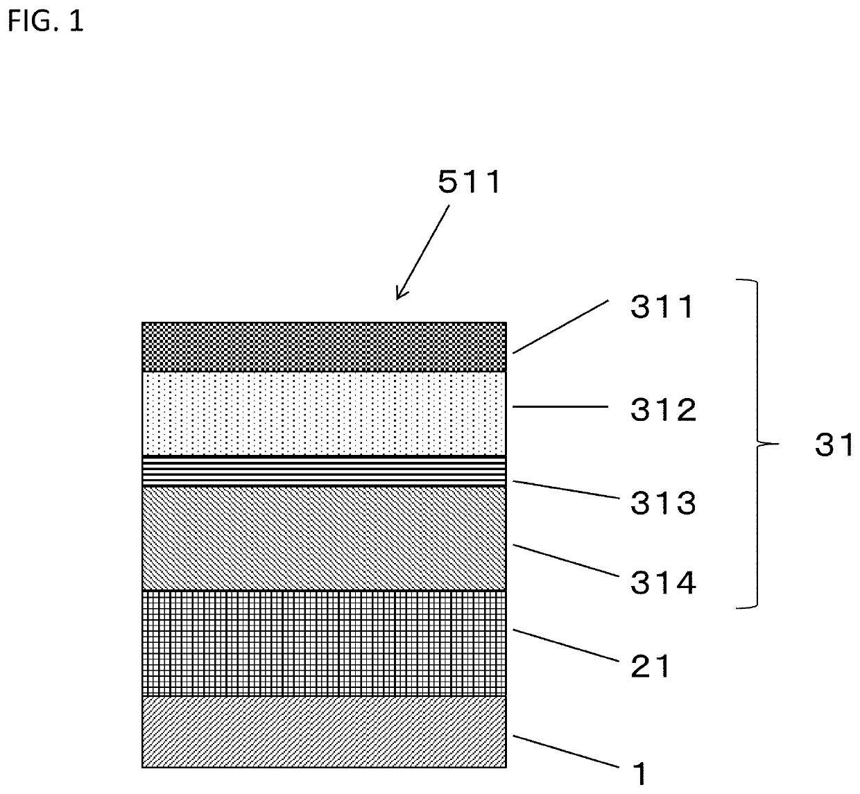
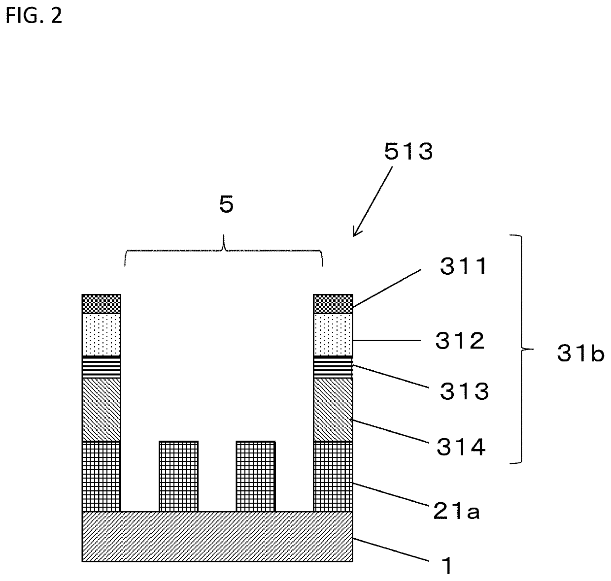
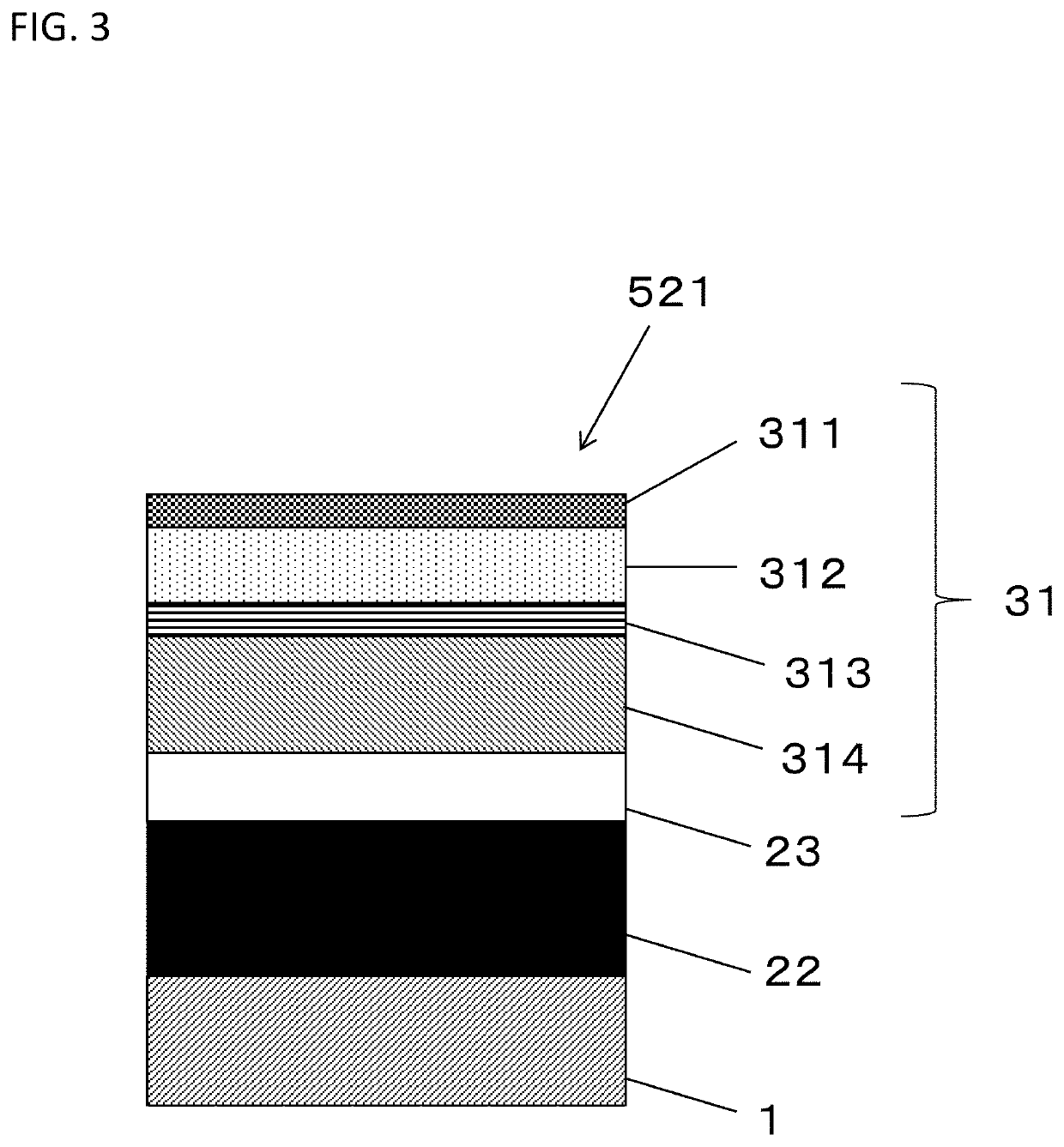
[0149]A photomask blank (halftone phase shift mask blank) was manufactured by laminating a phase shift film (halftone phase shift film) as a film made of a silicon-containing material on a transparent substrate made of quartz with a size of 152 mm square and a thickness of about 6 mm and a hard mask film as a film made of a chromium-containing material.

[0150]First, the power applied to the target was adjusted using a molybdenum target and a silicon target as a target on a transparent substrate, and sputtering was performed in these gas atmospheres using an argon gas and a nitrogen gas as a sputter gas, and a MoSi-based phase shift film, made of MoSiN, (thickness 70 nm) having a phase difference of 177 degrees and a transmittance of 6% (optical density 1.2) with respect to light having a wavelength of 193 nm was formed as a single-layer film.

example 2

[0151]Example 2 was the same as Example 1 except that the composition and thickness of each of the first layer, the second layer, the third layer, and the fourth layer of the hard mask film were changed so that the fourth layer of the hard mask film had reduced chromium atom %, and increased oxygen atom %, nitrogen atom %, and carbon atom %, compared with that of Example 1, and the optical density of the entire hard mask film was the same as that of Example 1, and a phase shift film and a hard mask film were formed on the transparent substrate to obtain a photomask blank without a resist film. A resist film was further formed on the hard mask film to obtain a photomask blank having a resist film. Table 1 shows the composition and thickness of each layer of the hard mask film, and the optical density of the entire hard mask film with respect to light having a wavelength of 193 nm.

example 3

[0152]Example 3 was the same as Example 1 except that the composition and thickness of each of the first layer, the second layer, the third layer, and the fourth layer of the hard mask film were changed so that the fourth layer of the hard mask film had reduced chromium atom %, and increased oxygen atom %, nitrogen atom %, and carbon atom %, compared with that of Example 1, and the optical density of the entire hard mask film was the same as that of Example 1, and a phase shift film and a hard mask film were formed on the transparent substrate to obtain a photomask blank without a resist film. A resist film was further formed on the hard mask film to obtain a photomask blank having a resist film. Table 1 shows the composition and thickness of each layer of the hard mask film, and the optical density of the entire hard mask film with respect to light having a wavelength of 193 nm.


PUM

PropertyMeasurementUnit
thicknessaaaaaaaaaa
thicknessaaaaaaaaaa
thicknessaaaaaaaaaa

Abstract

A photomask blank has a first layer, a second layer, a third layer and a fourth layer. The first layer has a chromium content of 40 atomic % or less, an oxygen content of 38 atomic % or more, and a nitrogen content of 22 atomic % or less. The second layer has a chromium content of 38 atomic % or less, an oxygen content of 30 atomic % or more, a nitrogen content of 18 atomic % or less, and a carbon content of 14 atomic % or less. The third layer has a chromium content of 50 atomic % or less, an oxygen content of 30 atomic % or less, and a nitrogen content of 20 atomic % or more. The fourth layer has a chromium content of 44 atomic % or less, an oxygen content of 20 atomic % or more, a nitrogen content of 20 atomic % or less, and a carbon content of 16 atomic % or less.

Description

TECHNICAL FIELD[0001]The present invention relates to a photomask blank used in the manufacture of a semiconductor device and the like, a method of manufacturing a photomask using the same, and a photomask.[0002]The present application claims the priority of Japanese Patent Application No. 2019-220060 filed on Dec. 5, 2019, the contents of which are entirely incorporated by reference.RELATED ART[0003]In recent years, with the miniaturization of semiconductor devices, particularly due to the high integration of large-scale integrated circuits, high pattern resolution is required for projection exposure. Therefore, in the photomask, a phase shift mask has been developed as a method of improving the resolution of the transfer pattern. In the principle of the phase shift method, by adjusting the phase of the transmitted light that has passed through the opening of the photomask so that it is inverted by about 180 degrees with respect to the phase of the transmitted light that has passed...

Claims


Application Information

Patent Timeline
Patent Type & Authority Patents(United States)
IPC IPC(8): G03F1/24G03F1/32G03F1/54G03F1/58G03F1/80H01L21/027H01L21/033
CPCG03F1/24G03F1/32G03F1/54G03F1/58G03F1/80H01L21/0274H01L21/0332H01L21/0337G03F1/22G03F1/50G03F1/68G03F1/62G03F1/38G03F1/26
Inventor MATSUHASHI, NAOKI
Owner SHIN ETSU CHEM IND CO LTD
Why Eureka
Try Eureka