Interface sensing membrane in bioelectronic device and method for forming the same

a bioelectronic device and sensing membrane technology, applied in the field of interface sensing membrane in a bioelectronic device and a, can solve the problems of not solving the problem, unable to maintain the immobilization of the bioelement, and the loss of the molecular recognition function of the bioelemen

Inactive Publication Date: 2001-07-26
LG ELECTRONICS INC
View PDF0 Cites 28 Cited by
  • Summary
  • Abstract
  • Description
  • Claims
  • Application Information

AI Technical Summary

Problems solved by technology

If the bioelement is happened to be brought into a direct contact with a solid state element of a metal or an inorganic material, there are problems caused in that the molecular recognition function of the bioelement is lost, losing the function as a bioelectronic device, and a nonspecific binding is caused by a non-reversible adsorption of an external biomaterial which is brought into contact with the interface of a surface of the device.
EP 254575 introduced a solvent casting technique in which a polymer, such as cellulose nitrate, is coated on a surface of a solid state element, for adsorbing, and immobilizing a bioelement on the surface of the solid state element, which however can not solve the problem of the nonspecific binding caused by other biomaterial in a sample.
However, though a precise adjustment of the immobilization location on the surface of the solid state element is possible, the foregoing methods have a problem in that there is a limitation in that the immobilization of the bioelement can not be maintained for a prolonged time period because the bioelement is immobilized by noncovalent bonding, which may cause a leak of the bioelement.
However, this method also has inconvenience of additional processing of a denaturant after the bioelement is immobilized for solving the problem caused by the nonspecific binding.
As discussed, the related art bioelement has problems in immobilizing the bioelement at a solid state element in that the bioelement is inactivated during an immobilization reaction, an activity of the bioelement is not stably maintained on the surface after the immobilization, or a non-specific binding of the other external biomaterials on the surface of the solid state element is caused.

Method used


Image

  • Interface sensing membrane in bioelectronic device and method for forming the same

Examples


embodiment 2

[0042] DNA interface, interaction between a DNA and a complementary DNA.

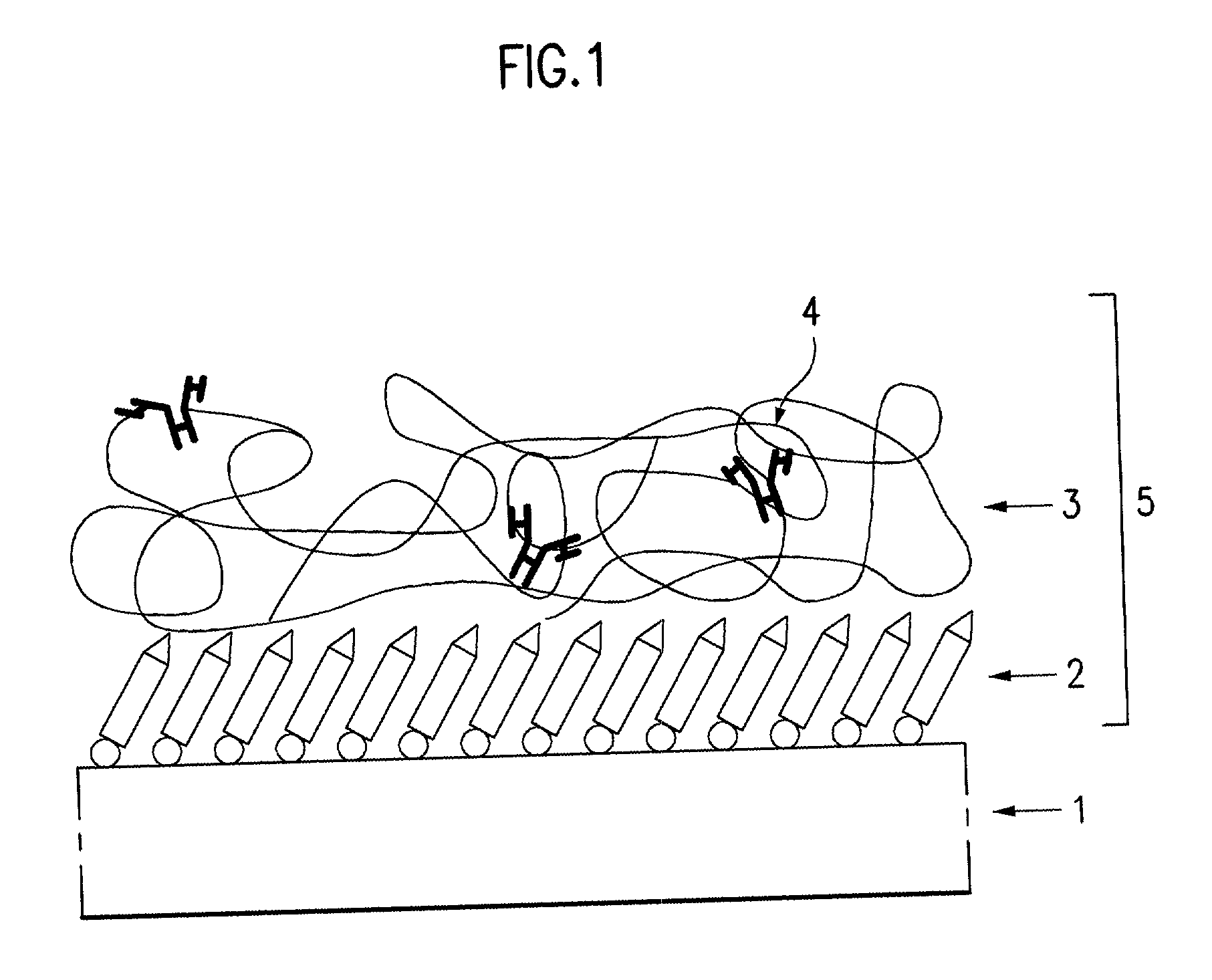
[0043] (1) Formation of a molecular adhesive layer on a gold thin film A process for forming the molecular adhesive layer on the gold thin film using a heterobifunctional reagent will be explained. A 3-mercaptopropionic acid(MPA) used as the heterobifunctional reagent has a thiol at one end and a carboxyl functional group at the other end. 1 mM of MPA solution is prepared using pure ethanol after deaeration by sonication. After 10 ml of the heterobifunctional reagent solution is filled in a glass scintillation vial, a specimen of the gold thin film is placed therein. Then, while being kept air tight, the vial is left standstill for more than 18 hours, to cause chemisorption reaction between the MPA solution and the gold thin film to form a molecular adhesive layer of a molecular monolayer. A surface of the molecular adhesive layer is washed with ethanol and water in succession, dried with nitrogen gas, and conse...

embodiment 3

[0048] (1) Formation of a molecular adhesive layer on a silicon chip

[0049] A process for forming a molecular monolayer processed with a heterobifunctional reagent as the molecular adhesive layer on the silicon chip will be explained. A (3-aminopropyl) trimethoxysilane(APS) used as the heterobifunctional reagent has a silane functional group at one end and an amine functional group at the other end. A silicon wafer is cleaned and cut into 1.times.1 cm.sup.2 size. A surface of the cut silicon chip is washed with anhydrous toluene containing 2% APS within a glove box kept air tight by an inert gas, such as argon, took out of the glove box, and dried by blowing nitrogen thereto. After the molecular monolayer is formed, the next step of formation of the hydrophilic three dimensional microstructured layer is started without delay.

[0050] (2) Formation of three dimensional micro structured layer on the molecular adhesive layer

[0051] The hydrophilic three dimensional microstructured layer ca...


PUM

PropertyMeasurementUnit
thicknessaaaaaaaaaa
resistanceaaaaaaaaaa
pHaaaaaaaaaa

Abstract

Interface sensing membrane in a bioelectronic device and a method for forming the same, the device including a molecular adhesive layer chemically adsorbed to a surface of a solid state element, a three dimensional microstructured layer of a hydrophilic polymer connected to the molecular adhesive layer in a covalent bond, and a bioelement immobilized in the three dimensional microstructured layer by covalent adhesive, whereby causing a stable biomolecular interaction.

Description

[0001] 1. Field of the Invention[0002] The present invention relates to an interface sensing membrane in a bioelectronic device and a method for forming the same, which is provided with a three dimensional microstructure for immobilizing a bioelement at a surface of a solid state element, for interfacing the surface of the solid state element and an outside of the bioelectronic device, i.e., for causing a biomolecular specific interaction within the three dimensional microstructure.[0003] 2. Background of the Related Art[0004] The bioelectronic device, an electronic device to which a bioelement is introduced, is used for diagnosis and analysis, and as a part of an entire circuitry system and the like in various industrial fields, such as medical measurements, food analysis, or environmental measurements. As a typical bioelectronic device, there is a protein-based memory using a bacteriorhodopsin, a DNA chip, or biosensor. A biosensor is a device or an apparatus which employs a molec...

Claims


Application Information

Patent Timeline
Patent Type & Authority Applications(United States)
IPC IPC(8): C12Q1/00G01N33/543
CPCG01N33/54366C12Q1/00
Inventor SHIN, MIN CHOLKIM, SEUNG RYEOLKIM, TAE HANLEE, KANG SHINLEE, WON YONGPARK, JE KYUN
Owner LG ELECTRONICS INC
Why Eureka
Try Eureka