

Thin film formation apparatus and method of manufacturing self-light-emitting device using thin film formation apparatus
a thin film, self-lighting technology, applied in mechanical vibration separation, nuclear engineering, nuclear elements, etc., can solve the problem of liquid clogging in the discharge portion and other problems
- Summary
- Abstract
- Description
- Claims
- Application Information
AI Technical Summary
Benefits of technology
Problems solved by technology
Method used
Image

Examples
embodiment 1
[0106] Embodiment 1
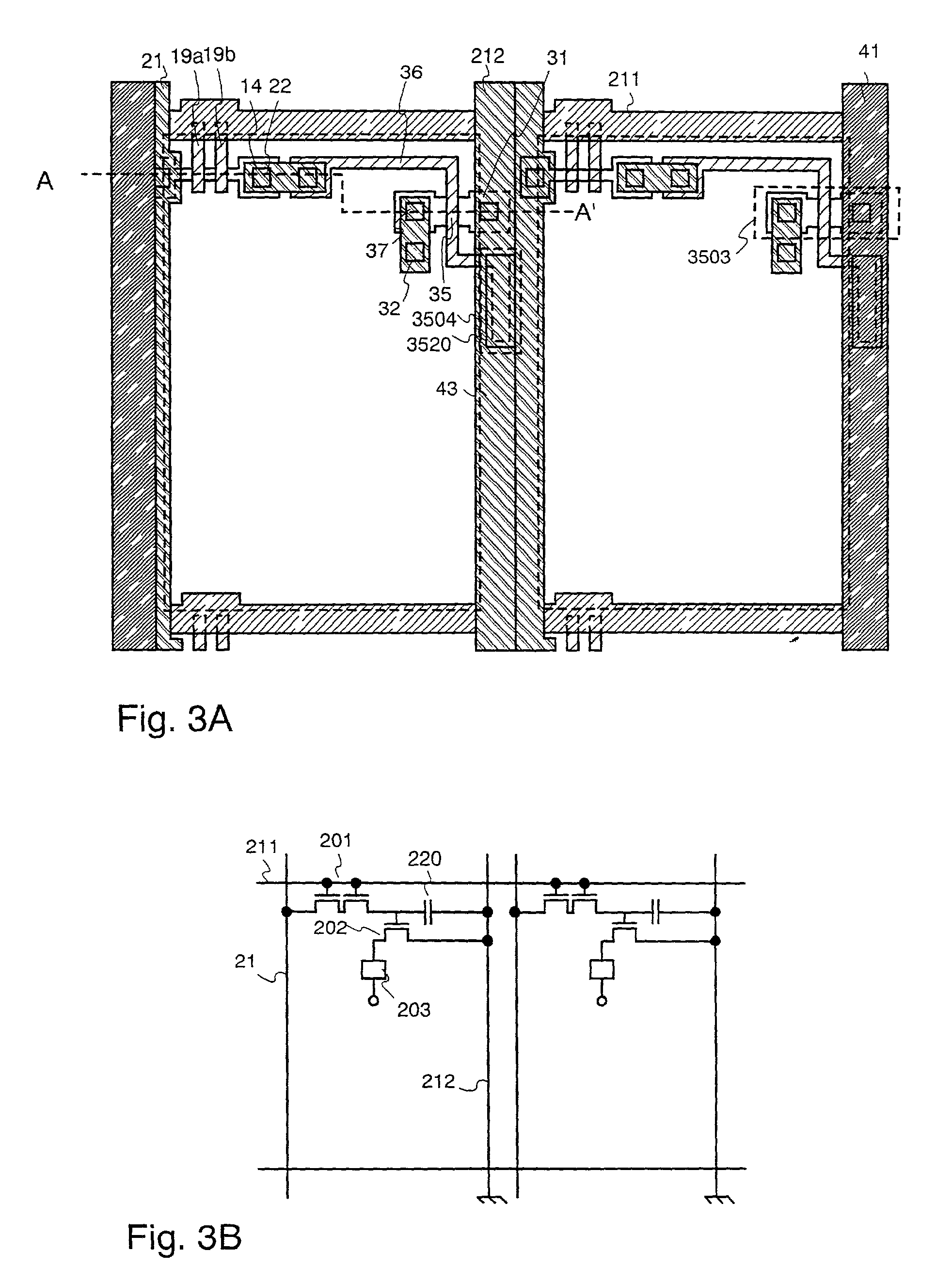
[0107] The embodiments of the present invention are explained using FIGS. 4A to 6C. A method of simultaneous manufacturing of a pixel portion, and TFTs of a driver circuit portion formed in the periphery of the pixel portion, is explained here. Note that in order to simplify the explanation, a CMOS circuit is shown as a basic circuit for the driver circuits.
[0108] First, as shown in FIG. 4A, a base film 301 is formed with a 300 nm thickness on a glass substrate 300. A 100 nm silicon oxynitride film and a 200 nm silicon oxynitride film are laminated as the base film 301 in embodiment 1. It is good to set the nitrogen concentration at between 10 and 25 wt % in the film contacting the glass substrate 300. Of course, an element can be formed on the carbon substrate directly without providing the base film.
[0109] Next, an amorphous silicon film (not shown in the figures) is formed with a thickness of 50 nm on the base film 301 by a known deposition method. Note that it...
embodiment 2
[0179] Embodiment 2
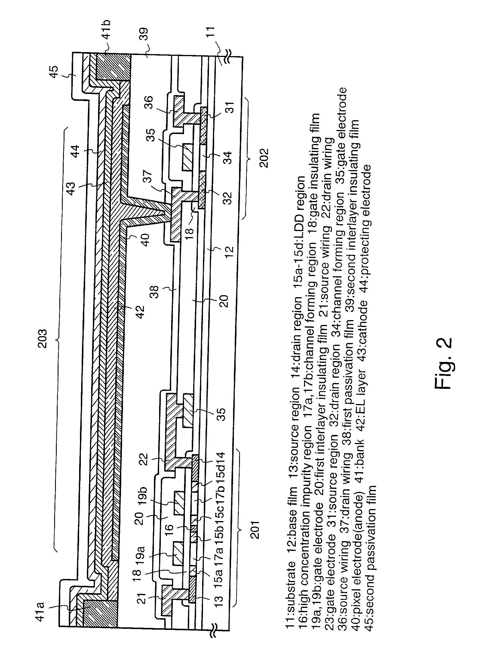
[0180] A method of manufacture which adds improvements to the contact structure in the pixel portion explained in FIG. 2 is explained next using the cross sectional diagrams of FIGS. 11A to 11C. Note that the reference numerals in FIGS. 11A to 11C correspond with the reference numerals in FIG. 2. A state in which the pixel electrode (anode) 40 structuring an EL element is obtained as shown in FIG. 11A, in accordance with the processes of Embodiment 1.
[0181] A contact portion 1900 on the pixel electrode is next filled in by acrylic, forming a contact hole protecting portion 1901, as shown in FIG. 11B.
[0182] Acrylic is formed into a film by spin coating here, and the contact hole protecting portion 1901 is formed as shown in FIG. 11B by performing etching after exposure using a resist mask.
[0183] Note that the contact hole protecting portion 1901 may have a thickness from 0.1 to 1 .mu.m, preferably from 0.1 to 0.5 .mu.m, and even better between 0.1 and 0.3 .mu.m, in...
embodiment 3
[0188] Embodiment 3
[0189] A pressurized type application method in which an application liquid is discharged onto a pixel portion from each nozzle by pressurizing the application liquid when implementing the present invention to form EL layers is shown in Embodiment 1. In Embodiment 3, an example of using a fountain pen type application method utilizing capillary action, in which each nozzle is made from one flexible, fine tube, and in which an application liquid is discharged onto a pixel portion in accordance with the contact element contacting a bank of the pixel portion is explained in Embodiment 3.
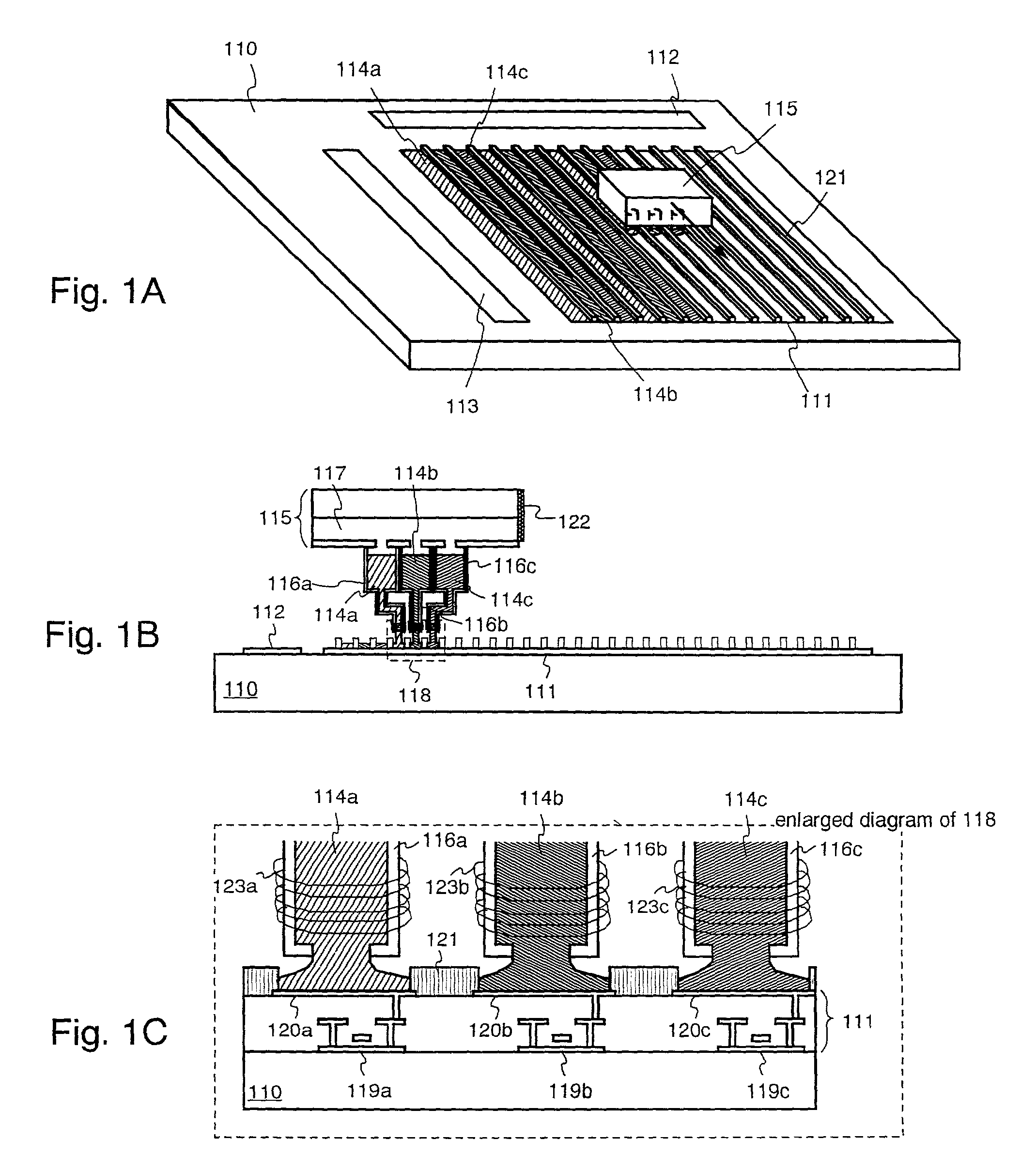
[0190] As shown in FIG. 13A the pixel portion 111, the source side driver circuit 112, and the gate side driver circuit 113 are formed on the substrate 110 by TFTs, and the pixel portion 111 is divided into stripe shapes by the banks 121.
[0191] A process of forming a film from an organic EL material, which functions as an EL layer using a thin film formation apparatus of FIG. 13 is pe...
PUM
| Property | Measurement | Unit |
|---|---|---|
| Weight | aaaaa | aaaaa |
| Pressure | aaaaa | aaaaa |
| Diameter | aaaaa | aaaaa |
Abstract
Description
Claims
Application Information