Optical filter construction by atomic layer control for next generation dense wavelength division multiplexer

a technology of atomic layer control and optical filter, which is applied in the direction of optical elements, polycrystalline material growth, instruments, etc., can solve the problems of cracking and delamination of coatings greater than 3.0 .mu.m thick, lack of thickness and roughness control, and intrinsic stress. compressive

Inactive Publication Date: 2002-01-10
ATOMIC TELECOM
View PDF4 Cites 36 Cited by
  • Summary
  • Abstract
  • Description
  • Claims
  • Application Information

AI Technical Summary

Benefits of technology

0016] An optical filter has been developed which uses, but is not limited to, alternating layers of high index materials such as titanium oxide (TiO.sub.2, n=2.2 @ 1.55 .mu.m ), amorphous silicon (Si, n=3.46 @ 1.55 .mu.m), and tantalum pentoxide (Ta.sub.2O.sub.5, n=2.05 @ 1.55 .mu.m), and low index materials such as silicon dioxide (SiO.sub.2, n=1.45 @ 1.55 .mu.m) and magnesium fluoride (MgF.sub.2, n=1.35 @ 1.55 .mu.m), to enable next generation multiplexers and demultiplexers for DWDM systems. The optical filter is unique in that it uses atomic layer deposition processes commonly used in the semiconductor industry and a Chemical Reactive-Ion Surface Planarization (CRISP) process to produce atomically smooth (R.sub.a<0.01 nm) interfaces. The filter will enable narrow bandpass filters of 12.5 GHz with the necessary environmental stability to construct next generation optical communications hardware.

Problems solved by technology

Filters produced with these processes are stable under adverse environmental conditions but lack necessary thickness and roughness control to multiplex / demultiplex more than 80 channels in the desired wavelength range.
Intrinsic stress is compressive and can be quite high ultimately leading to cracking and delamination in coatings greater than 3.0 .mu.m thick.

Method used


Image

  • Optical filter construction by atomic layer control for next generation dense wavelength division multiplexer
  • Optical filter construction by atomic layer control for next generation dense wavelength division multiplexer

Examples


Embodiment Construction

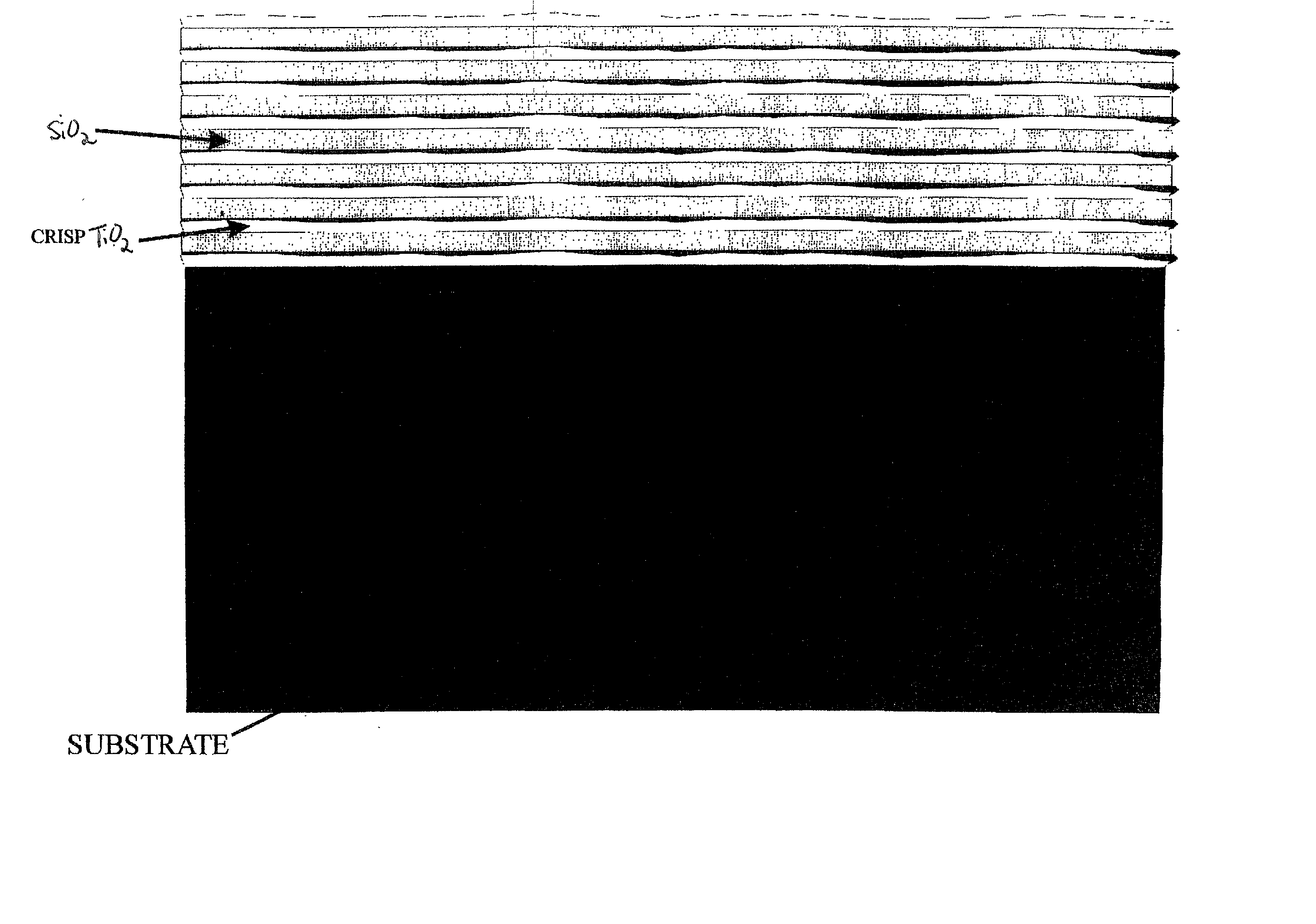
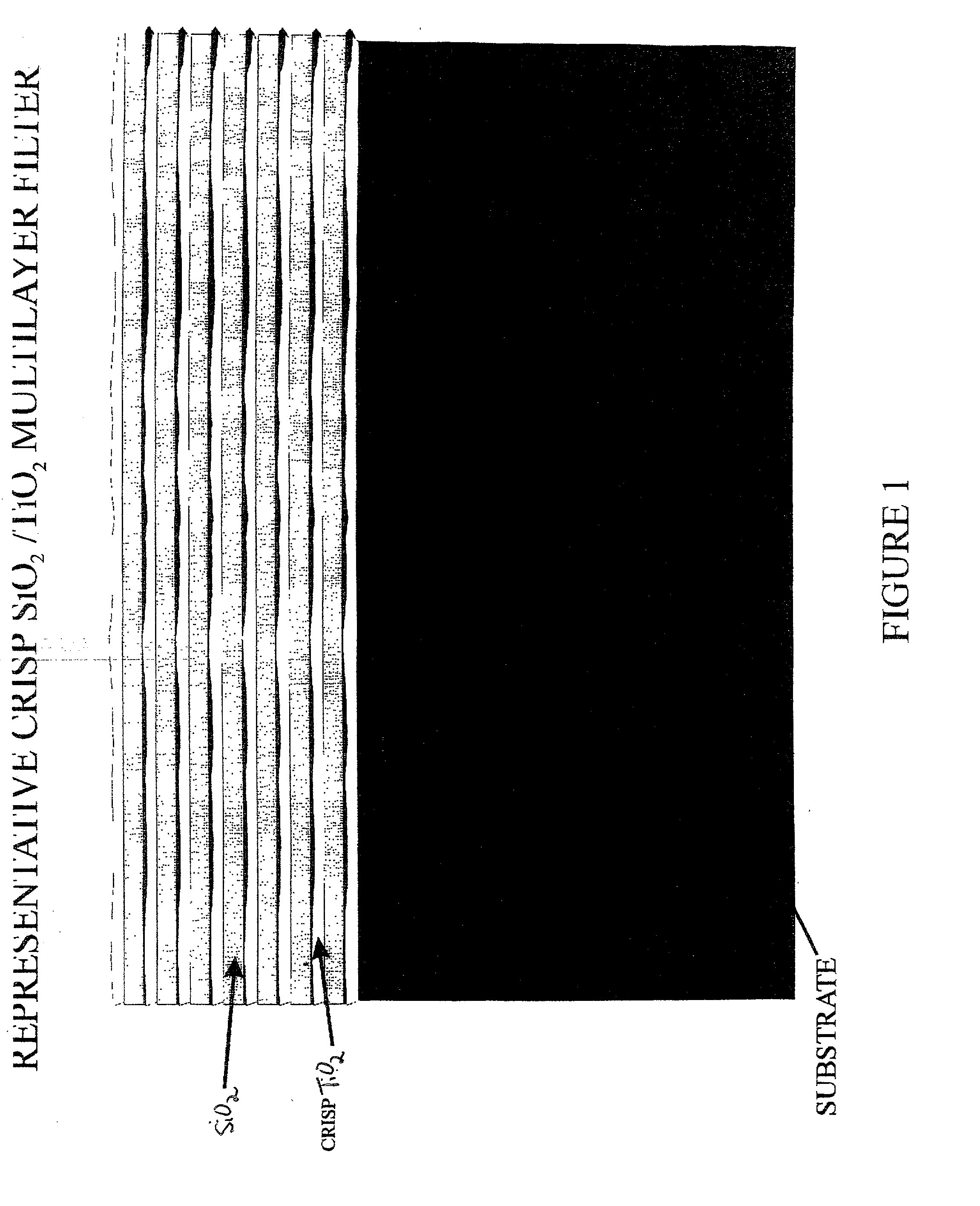
[0026] Referring now to the drawings, which are for purposes of illustrating at least one embodiment of the invention only, and not for purposes of limiting the invention, FIG. 1 shows an optical filter which uses alternating layers of high index materials such as, but not limited to, titanium dioxide (TiO.sub.2, n=2.2 @ 1.55 .mu.m), amorphous silicon (Si, n=3.46 @ 1.55 .mu.m), and tantalum pentoxide (Ta.sub.2O.sub.5, n=2.05 @ 1.55 .mu.m), and low index materials such as, but not limited to, silicon dioxide (SiO.sub.2, n=1.45 @ 1.55 .mu.m) and magnesium fluoride (MgF.sub.2, n=1.35 @ 1.55 .mu.m).

[0027] The high index layers are grown with a self-limiting deposition process, which include, but are not limited to, atomic layer epitaxy (ALE), pulsed chemical beam epitaxy (PCBE), molecular layer epitaxy (MLE), or molecular beam epitaxy (MBE), which can result in layer-by-layer growth. In some cases a polycrystalline or amorphous layer will grow but the atomic layer control is maintained....


PUM

PropertyMeasurementUnit
thickaaaaaaaaaa
surface roughnessaaaaaaaaaa
FWHMaaaaaaaaaa

Abstract

An optical filter using alternating layers of materials with "low" and "high" indices of refraction and deposited with atomic layer control has been developed. The multilayered thin film filter uses, but is not limited to, alternating layers of single crystal, polycrystalline or amorphous materials grown with self-limiting epitaxial deposition processes well known to the semiconductor industry. The deposition process, such as atomic layer epitaxy (ALE), pulsed chemical beam epitaxy (PCBE), molecular layer epitaxy (MLE) or laser molecular beam epitaxy (laser MBE) can result in epitaxial layer by layer growth and thickness control to within one atomic layer. The alternating layers are made atomically smooth using the patent pending Chemical Reactive-Ion Surface Planarization (CRISP) process. Intrinsic stress is monitored using an in-situ cantilever-based intrinsic stress optical monitor and adjusted during filter fabrication by deposition parameter modification. The resulting filter has sufficient individual layer thickness control and surface roughness to enable ~12.5 GHz filters for next generation multiplexers and demultiplexers with more than 1000 channels in the wavelength range 1.31-1.62 mum.

Description

I. BACKGROUND OF THE INVENTION[0001] A. Field of the Invention[0002] This application claims priority to U.S. Provisional Patent Application Ser. No. 60 / 206,934, entitled OPTICAL FILTER CONSTRUCTION BY ATOMIC LAYER CONTROL FOR NEXT GENERATION DENSE WAVELENGTH DIVISION MULTIPLEXER, filed on May 25, 2000, U.S. Provisional Patent Application Ser. No. 60 / 207,100, entitled ATOMIC LAYER CONTROLLED OPTICAL FILTER DESIGN FOR NEXT GENERATION DENSE WAVELENGTH DIVISION MULTIPLEXER, filed on May 25, 2000, and U.S. Provisional Patent Application Ser. No. 60 / 207,101, entitled CHEMICAL-ORGANIC PLANARIZATION PROCESS FOR ATOMICALLY SMOOTH INTERFACES, filed on May 25, 2000. The present invention relates to an oxygen ion process called Chemical Reactive-Ion Surface Planarization (CRISP) which reduces the surface roughness of thin film surfaces at the atomic level.[0003] B. Description of the Related Art[0004] The present invention contemplates a new and improved process for reducing the surface roughn...

Claims


Application Information

Patent Timeline
Patent Type & Authority Applications(United States)
IPC IPC(8): C23C14/54C23C16/56
CPCC23C14/547C23C16/56
Inventor MEARINI, GERALD T.TAKACS, LASZLO
Owner ATOMIC TELECOM
Why Eureka
Try Eureka