Method for forming a refractive-index-patterned film for use in optical device manufacturing

Inactive Publication Date: 2002-04-25
PHOSISTOR TECH
View PDF0 Cites 19 Cited by
  • Summary
  • Abstract
  • Description
  • Claims
  • Application Information

AI Technical Summary

Problems solved by technology

Such conventional multi-step processes can be expensive and complicated.
However, the photosensitive polymer films used in such conventional processes suffer from several drawbacks, such as (i) polymer instability; (ii) undesirable

Method used


Image

  • Method for forming a refractive-index-patterned film for use in optical device manufacturing
  • Method for forming a refractive-index-patterned film for use in optical device manufacturing
  • Method for forming a refractive-index-patterned film for use in optical device manufacturing

Examples


Embodiment Construction

[0019] To be consistent throughout the present specification and for clear understanding of the present invention, the following definition is hereby provided for a term used therein:

[0020] The term "refractive-index-patterned film" refers to a film (e.g., a lead-silicate-containing film) that includes at least one film portion of a predetermined pattern (design), whose refractive index was modified (i.e., increased or decreased) following formation of the film.

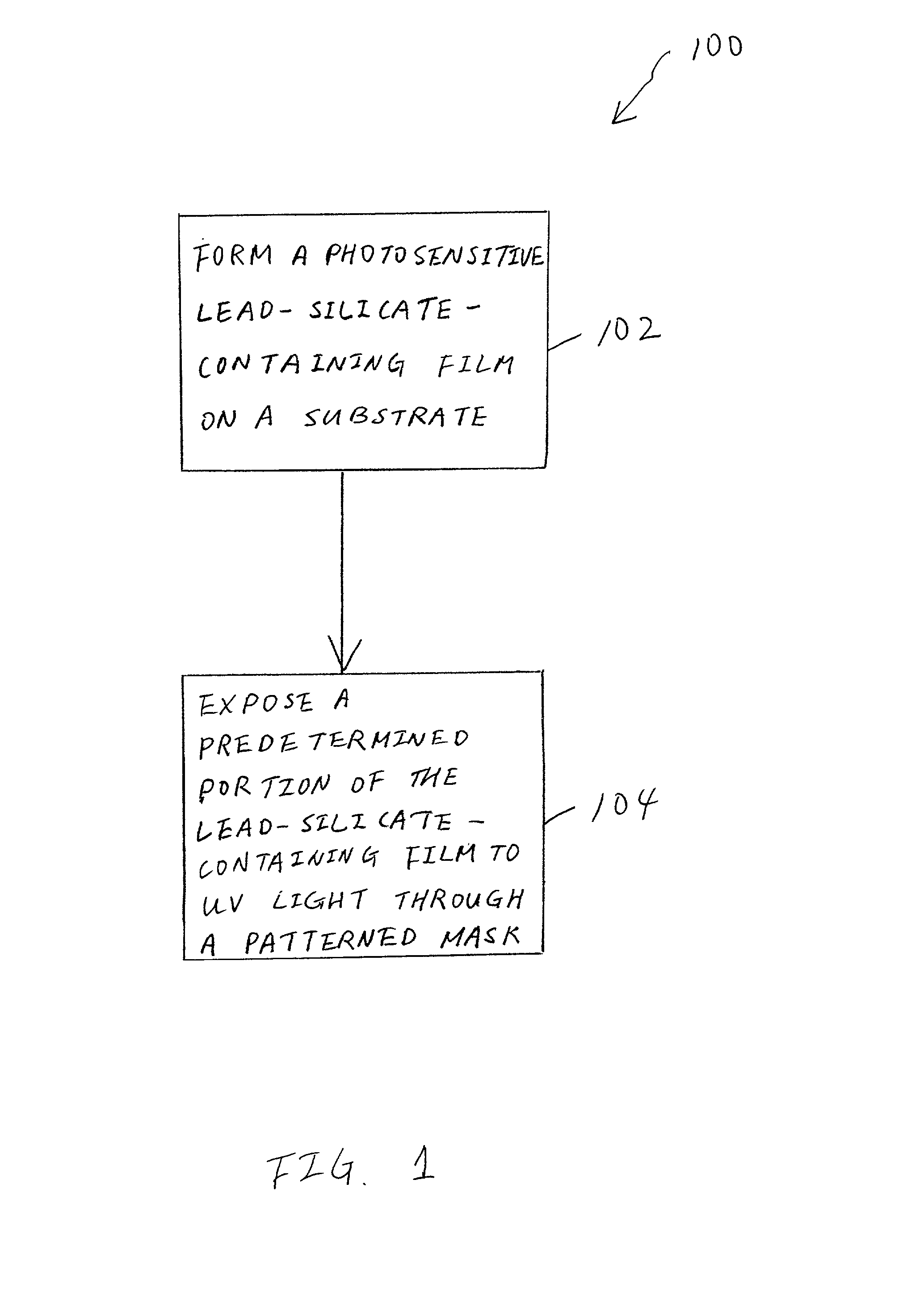
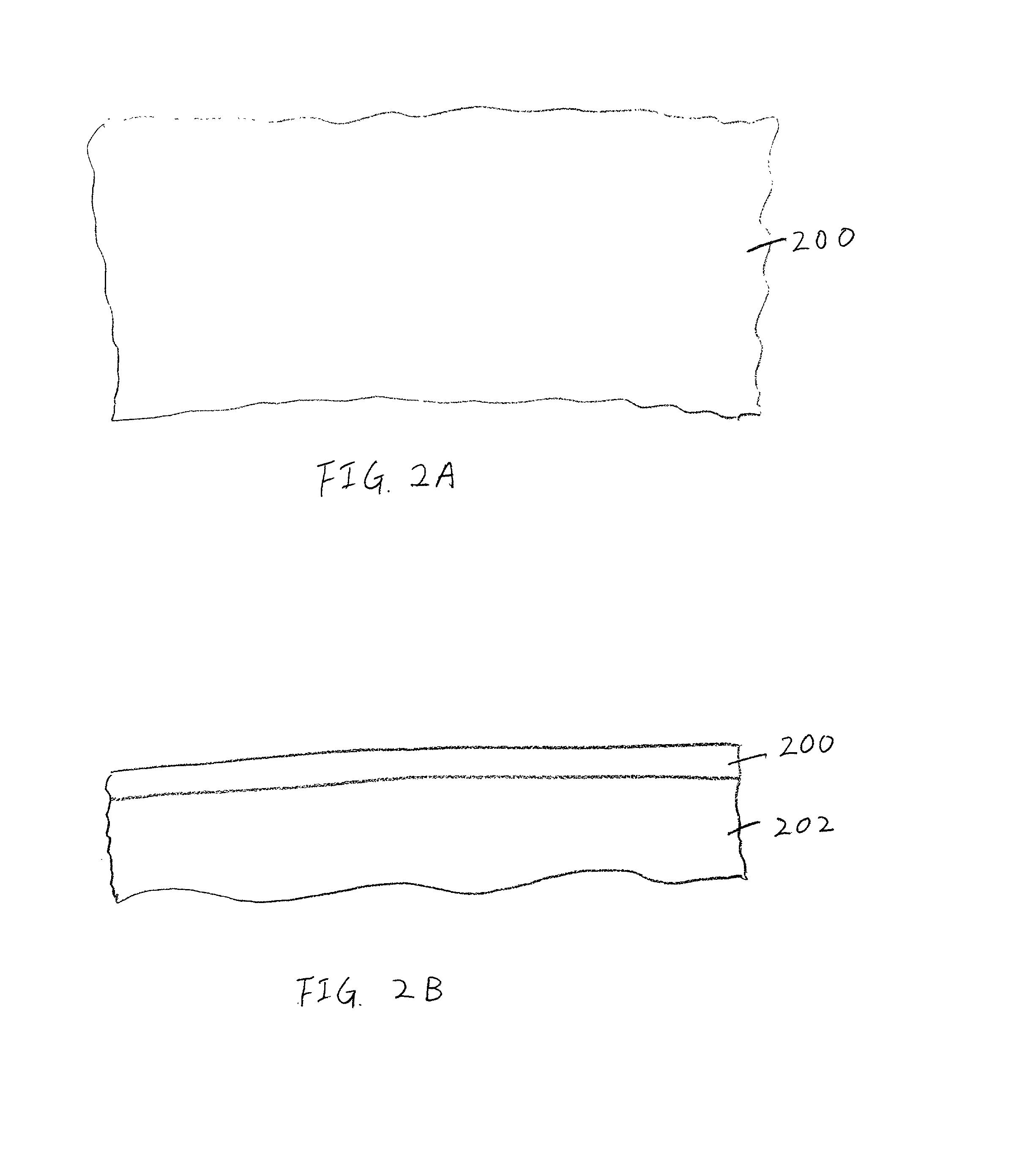
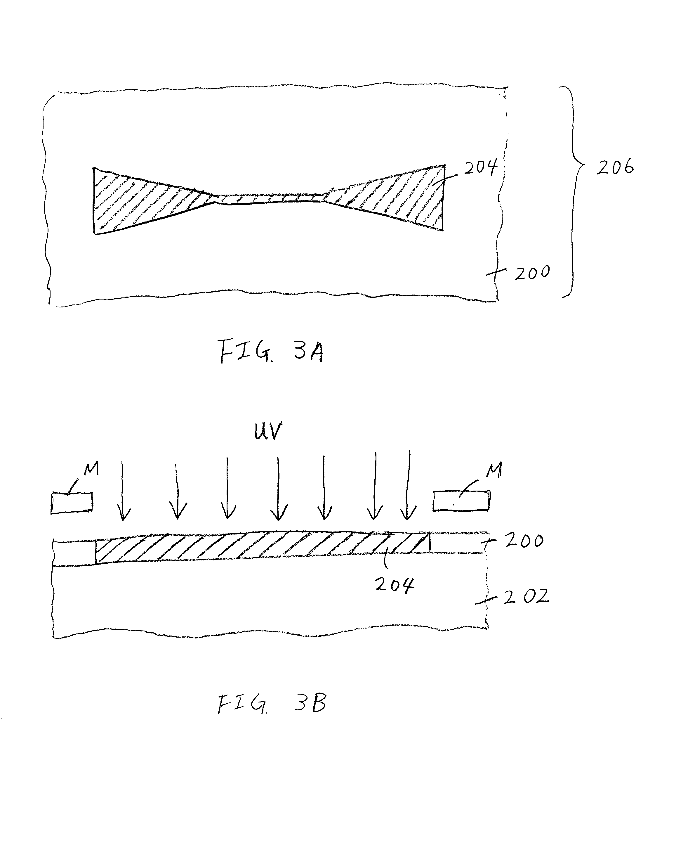
[0021] Process 100 includes first forming a photosensitive lead-silicate-containing film 200 on a substrate 202, as illustrated at step 102 of FIG. 1 and in FIGS. 2A-2B. Substrate 202 can be any suitable substrate known to those skilled in the art. For example, substrate 202 can be a quartz, silica-on-silicon, gallium arsenide (GaAs), indium phosphide (InP), gallium nitride (GaN), lithium niobate (LiNbO.sub.3), barium titanate (BaTiO.sub.3) or sapphire (Al.sub.2O.sub.3) substrate.

[0022] Photosensitive lead-silicate-containing...


PUM


Abstract

A process for forming a refractive-index-patterned film for use in optical device manufacturing. The process includes forming a photosensitive lead-silicate-containing film on a substrate (e.g., a silicon, quartz or glass substrate) using, for example, a conventional and inexpensive sol-gel process. A predetermined portion of the lead-silicate-containing film is subsequently exposed to ultra-violet (UV) light through a patterned mask (e.g., a patterned amplitude mask, patterned phase mask or patterned gray scale mask). The UV exposure modifies the refractive index of the predetermined portion, thereby forming a refractive-index-patterned lead-silicate-containing film suitable for use in optical device manufacturing. The use of a photosensitive lead-silicate-containing film enables a relatively large refractive index modification upon exposure to UV light. A vertically tapered waveguide region that includes a substrate with a sloped upper surface protrusion and a refractive-index-patterned lead-silicate-containing film can be formed using the above described process. The refractive-index-patterned lead-silicate film is disposed on the substrate and sloped upper surface protrusion and is, therefore, vertically tapered (i.e., thinned) over the sloped upper surface protrusion. PATENT

Description

CROSS-REFERENCES TO RELATED APPLICATIONS[0001] This application claims priority from U.S. provisional application No. 60 / 242,188, filed Oct. 20, 2000, which is hereby fully incorporated by reference.[0002] 1. Field of the Invention[0003] The present invention relates, in general, to optical device manufacturing and, in particular, to methods for forming refractive-index-patterned films.[0004] 2. Description of the Related Art[0005] The manufacturing of optical devices and circuits (e.g., optical gratings, integrated photonic circuits and opto-electronic devices / circuits) typically requires a process for forming a device region (e.g., an integrated waveguide region) with a refractive index that differs from adjacent device regions. Conventional processes for the formation of integrated waveguide regions involve the use of multi-step techniques combining deposition, photolithography, etching, diffusion or ion implantation. Such conventional multi-step processes can be expensive and co...

Claims


Application Information

Patent Timeline
IPC IPC(8): G02B6/122G02B6/13
CPCG02B6/13G02B6/1228
Inventor ZHOU, YANHO, SENG-TIONG
Owner PHOSISTOR TECH
Why Eureka
Try Eureka