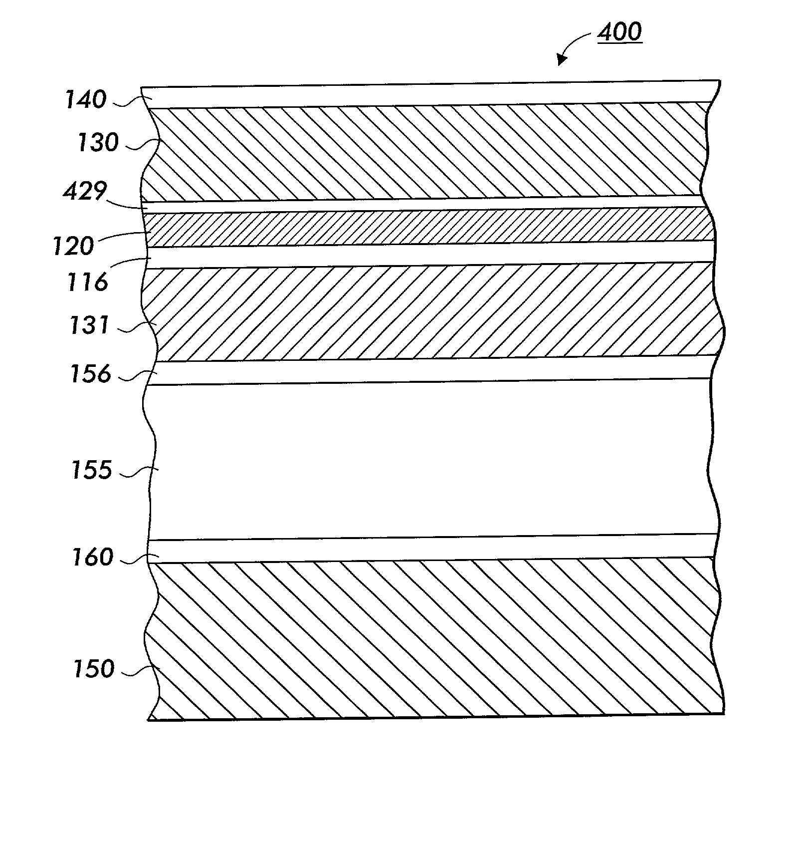
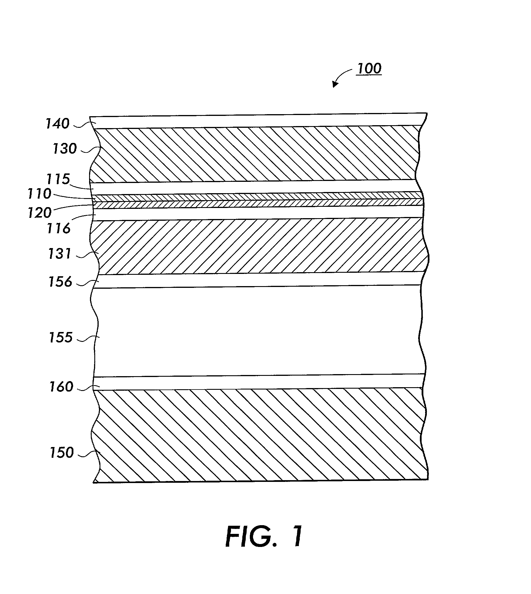
[0008] In accordance with the present invention, a p-type cladding layer is used to eliminate the p-type
waveguide and eliminate the need for a p-type, very high bandgap, high-aluminum content AlGaN
tunnel barrier layer in nitride laser diodes. The p-type cladding layer is used to suppress
electron leakage. In addition to the p-type cladding layer, a high-Al-content
tunnel barrier, a
superlattice structure or a distributed
electron reflector may be placed at the
multiple quantum well region / p-cladding
layer interface. Although a p-type cladding layer is used for suppressing
electron leakage in laser diodes fabricated from other materials such as arsenides and phosphides, the use of p-cladding layer in nitride laser diodes is not straightforward. The minority carrier
diffusion lengths (average distance minority carrier travels before recombination occurs) in nitrides are many times shorter than in other
laser diode materials. Hence, the p-cladding layer typically lies several
diffusion lengths away from the multiple-
quantum well active region. Consequently, injected electrons are not appreciably confined by the p-cladding layer which leads to the requirement for the high-aluminum content tunnel
barrier layer. In red and
infrared laser diodes, the waveguide thickness is a mere fraction of the
diffusion length, so that the cladding layer can effectively suppress leakage, see for example, "Drift leakage current in AlGaInP
quantum well laser diodes," D. P. Bour, D. W. Treat, R. L. Thomton, R. S. Geels, and D. F. Welch, IEEE Journal of
Quantum Electronics, vol. 29, pp. 1337-1343 (1993).
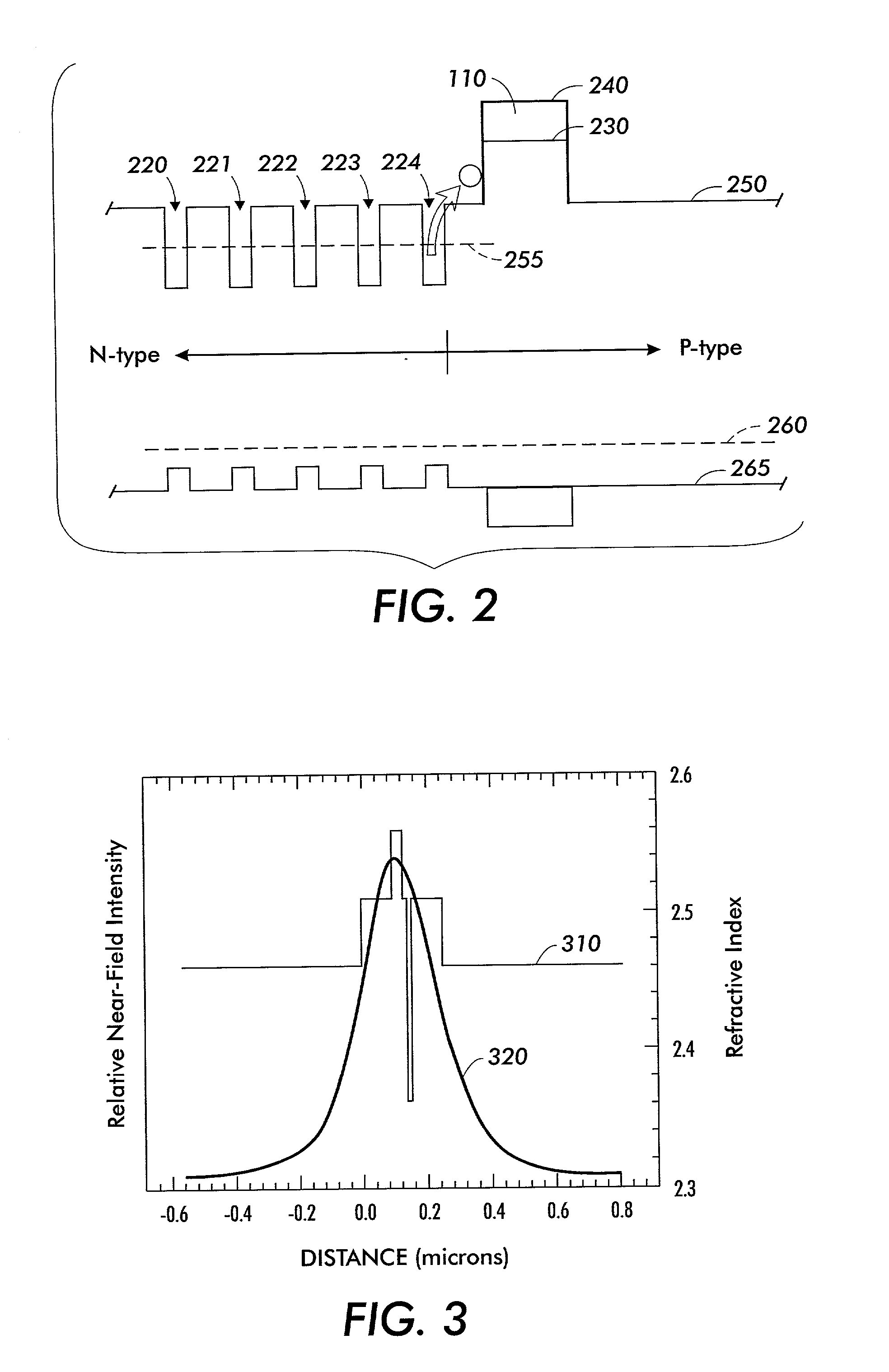
[0010] A
superlattice may be introduced into the asymmetric waveguide nitride
laser diode structure or a conventional nitride laser structure to enhance carrier confinement. The
superlattice is used to replace a uniform bulk layer. A properly designed superlattice inhibits the tendency for structural defect formation while allowing adequate p-type
doping and carrier confinement in the
quantum wells. For example, a superlattice that alternates GaN with AlGaN
layers allows high p-
doping since the GaN
layers are readily p-doped. Carrier confinement requires adequate band offsets in the valence and conduction bands between the
quantum well active region and the surrounding
layers. Carrier confinement by superlattice structures also requires avoiding resonant tunneling effects.
[0011] Short period superlattices may be designed to act as coherent electron reflectors. Short period superlattices function as distributed Bragg reflectors which reflect the wavefunction of leaked electrons back into the
multiple quantum well active region. Similar structures, often called "Multi-
Quantum Barriers" are used to confine electrons in short
wavelength (.
lambda.<650 nm) red AlGaNInP lasers where they are placed in the p-cladding layer rather than immediately next to the
multiple quantum well active region. As coherent reflections may be produced using low-bandgap superlattice layers, the need for AlGaN layers may be reduced or eliminated. This preserves the structural quality of films while transverse waveguiding is not negatively effected by AlGaN layers and p-type
doping benefits from the ability to use low-bandgap barrier layers. The thickness of the layers making up the superlattices needs to be selected to avoid resonant tunneling. Appropriate selection of layer thicknesses allows an electron
reflectivity of about 100% for electron energies beyond the classical barrier height. Therefore, properly designed distributed electron reflectors may be more effective than bulk barrier layers for confining injected electrons.
[0012] Hence, in accordance with the present invention, nitride
laser diode structures can be made which eliminate the need for the p-type waveguide layer and the high-aluminum-content tunnel barrier and have a p-cladding layer deposited above the multiple
quantum well active region to confine electrons. Additionally, superlattices may be introduced between the multiple
quantum well region and the p-cladding layer to enhance carrier confinement.

