
Method for manufacturing thin film transistor array panel for liquid crystal display

a technology of thin film transistors and array panels, which is applied in the direction of identification means, instruments, optics, etc., can solve the problems of complex manufacturing process, difficult method implementation, and inability to stand up to physical and chemical variations,

Inactive Publication Date: 2002-05-30
SAMSUNG ELECTRONICS CO LTD
View PDF0 Cites 72 Cited by
  • Summary
  • Abstract
  • Description
  • Claims
  • Application Information

AI Technical Summary

Benefits of technology

[0012] It is the other object of the present invention to prevent the LCD's current leakage.

Problems solved by technology

Even though a few manufacturing methods using only four photolithography steps are suggested, these methods are not easy to accomplish.
The aluminum and the aluminum alloy cannot stand against physical and chemical variations and are vulnerable to damage and oxidation, despite their advantages of low resistivity.
However, the former makes the manufacturing process complicated, and the latter may result in a high resistivity problem.

Method used


Image

  • Method for manufacturing thin film transistor array panel for liquid crystal display
  • Method for manufacturing thin film transistor array panel for liquid crystal display
  • Method for manufacturing thin film transistor array panel for liquid crystal display

Examples


fourth embodiment

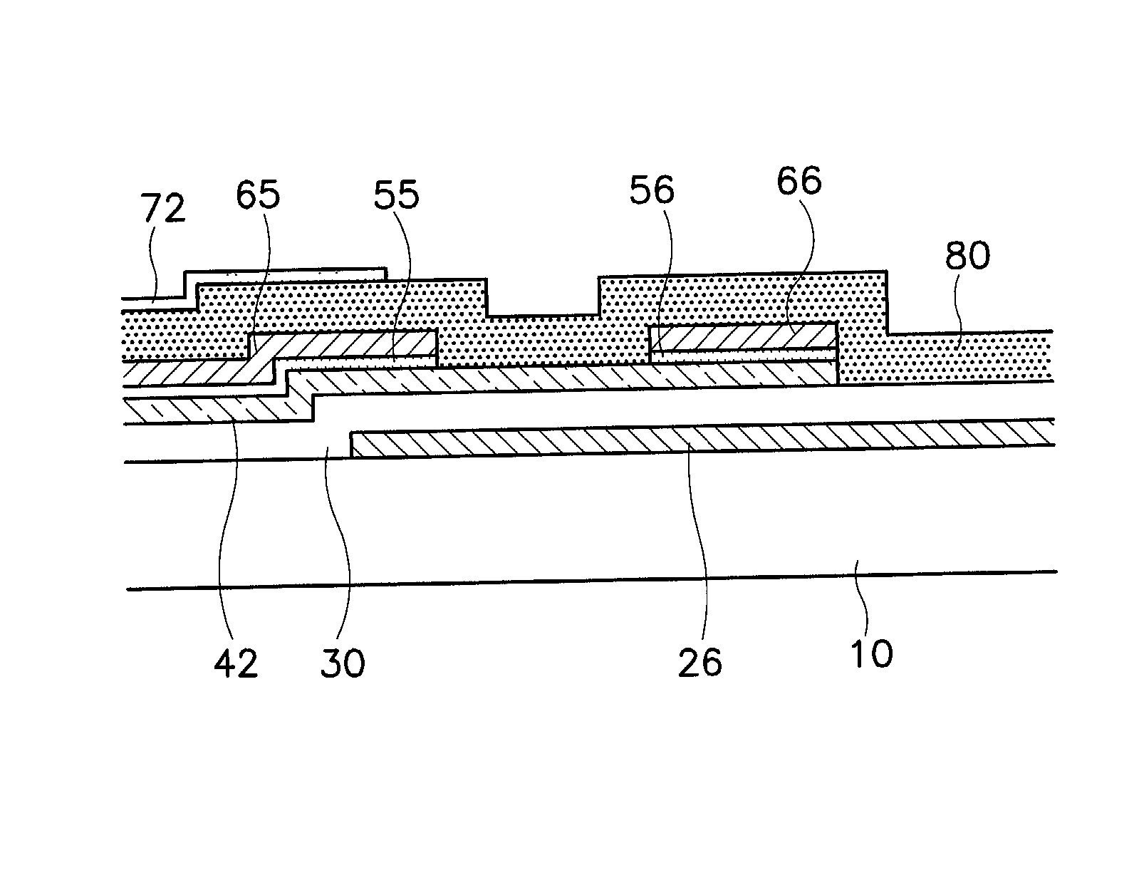
[0100] A passivation layer 80 made of insulating material such as SiNx is formed on the described structure, and has a plurality of openings 83, 84 and 85 respectively exposing the pixel electrode 71 and the third and the fourth pattern 73 and 74 of transparent conductor and openings 81 and 82 exposing the gate insulating layer 30. The openings 81 and 82 separate the semiconductor layer into two portions 42 and 47. It is to prevent a parasitic transistor of the gate line 22 as a gate, the date line 62 as a source and the pixel electrode 71 as a drain from being formed, as shown in FIG. 5. Since, in a previous gate type LCD like the present embodiment, where the pixel electrode 71 is overlapped with the previous gate line, such a parasitic transistor can cause a big problem. On the other hand, the semiconductor layer may form an electrical channel when voltages applied. The two adjacent data lines connected via a semiconductor layer may interfere the signals of the two data lines wit...

first embodiment

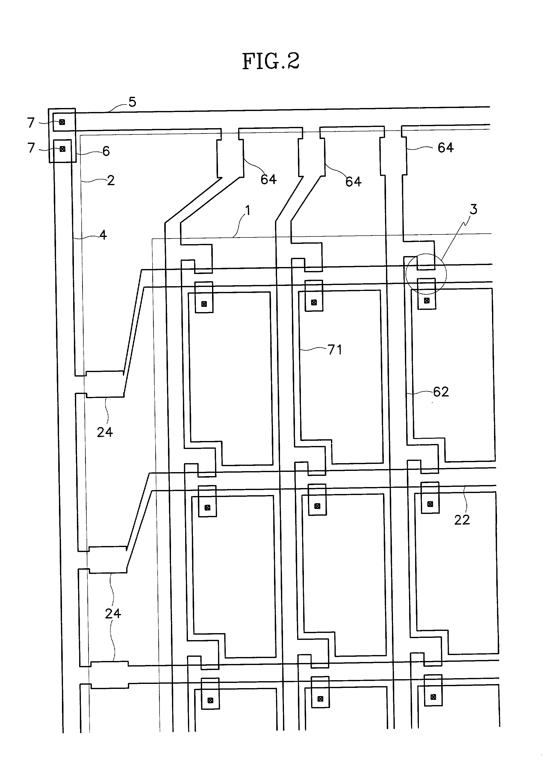
[0101] Now, a manufacturing method of a thin film transistor array panel according to the present invention will be described with reference to the FIGS. 6A to 8C and FIGS. 3 to 5 mentioned above.

[0102] FIGS. 6A, 7A and 8A are layout views of a TFT panel and are sequentially arranged according to the manufacturing step of the first embodiment of the present invention. FIGS. 6B, 6C, 7B, 7C, 8B and 8C are respectively the cross-sectional views taken along the line VIB-VIB' and VIC-VIC' of the FIG. 6A, VIIB-VIIB' and VIIC-VIIC' of the FIG. 7A and VIIIB-VIIIB' and VIIIC-VIIIC' of the FIG. 8A.

[0103] At first, as shown in FIGS. 6A to 6C, a conductor layer is deposited on a substrate 10 by such methods as sputtering to have a thickness 1,000 .ANG. to 3,000 .ANG., and a gate wire including a gate line 22, a gate pad 24 and a gate electrode 26 is formed by dry etch or wet etch using the first mask. As described above, the gate wire 22, 24 and 26 may be formed of double layers of Al--Nd and M...

second embodiment

[0108] A TFT array panel and a manufacturing method thereof according to the present invention will be described.

[0109] FIG. 9 is a layout view of a TFT panel for an LCD according to the second embodiment of the present invention and an enlarged view of a portion mainly including a pixel and pads of the FIG. 2, and FIGS. 10 and 11 are cross-sectional views respectively taken along the line X-X' and XI-XI' of the FIG. 9.

[0110] As shown in FIGS. 9 to 11, the structure of the TFT array panel of the second embodiment is almost the same as that of the first embodiment except for that around the pads. That is to say, between the pads, the gate insulating layer 30 is removed in the first embodiment, but is not removed in the second embodiment. In addition, in the second embodiment, the passivation layer 80 has an opening 86 marked as slanted creases, exposing the gate insulating layer 30 between the pads. Therefore, the pads are not connected to each other through the semiconductor layer.

[...


PUM


Abstract

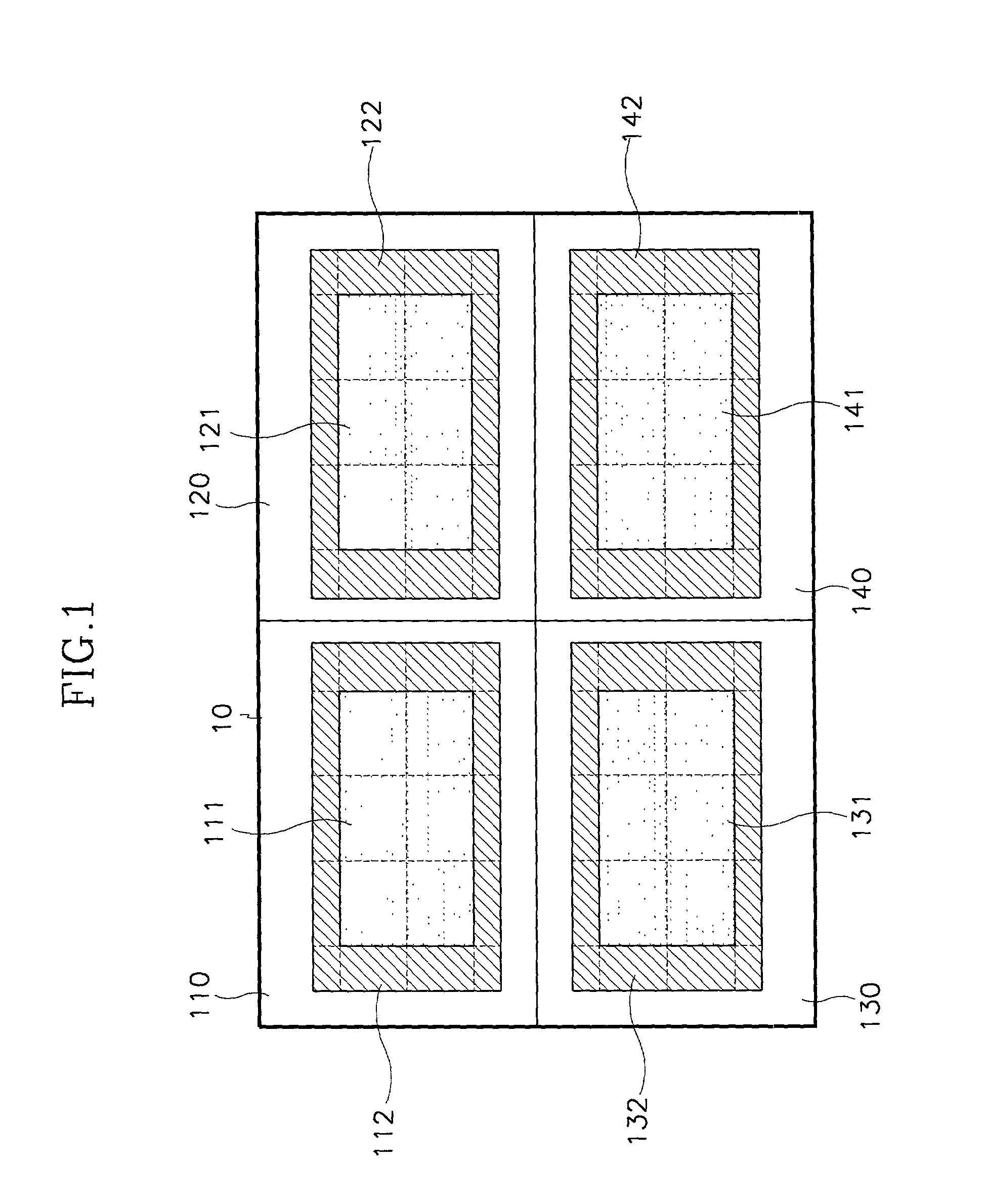
Simplified method of manufacturing liquid crystal displays. A gate wire including a gate line, a gate pad and a gate electrode is formed on the substrate by using the first mask. A gate insulating layer, a semiconductor layer, a ohmic contact layer and a metal layer are sequentially deposited to make a quadruple layers, and patterned by a dry etch of using the second mask. At this time, the quadruple layers is patterned to have a matrix of net shape layout and covering the gate wire. An opening exposing the substrate is formed in the display area and a contact hole exposing the gate pad is formed in the peripheral area. Next, ITO is deposited and a photoresist layer coated on the ITO. Then, the ITO layer is patterned by using the third mask and a dry etch, and the data conductor layer and the ohmic contact layer not covered by the ITO layer is dry etched. After depositing a passivation layer, a opening is formed by using the fourth mask and the exposed semiconductor layer through the opening is etched to separate the semiconductor layer under the adjacent data line.

Description

[0001] (a) Field of the Invention[0002] The present invention relates to a thin film transistor array panel for a liquid crystal display and a method for manufacturing the same, especially to a method for manufacturing a thin film transistor array panel with a reduced number of photolithography steps.[0003] (b) Description of the Related Art[0004] A liquid crystal display (LCD) is one of the most popular FPDs (flat panel displays). The LCD has two panels having electrodes for generating electric fields and a liquid crystal layer interposed therebetween. The transmittance of incident light is controlled by the intensity of the electric field applied to the liquid crystal layer.[0005] In the most widely used LCD, the field-generating electrodes are provided at both panels, and one of the panels has switching elements such as thin film transistors (TFTs).[0006] In general, a thin film transistor array panel is manufactured by photolithography using a plurality of photomasks, and five o...

Claims


Application Information

Patent Timeline
IPC IPC(8): G02F1/136G02F1/1362G02F1/1368H01L21/336H01L29/417H01L29/786G09F9/30
CPCG02F1/13458G02F1/1362G02F1/136227G02F2001/136236H01L27/12H01L27/1288H01L29/458Y10S438/947Y10S438/949Y10S438/942H01L27/124H01L29/41733G02F1/136236
Inventor HONG, MUN-PYOPARK, WOON-YONGYOON, JONG-SOO
Owner SAMSUNG ELECTRONICS CO LTD
Learn More